
دانلود رایگان مقاله ویژگی ساختاری SnS خالص و لایه های نازک ایندیم
چکیده:
یک مسیر الکتروشیمیایی برای تهیه لایه های نازک ایندیم-آلاییده SnS و خالص SnS استفاده شده است. شش نمونه شامل لایه های نازک ایندیم-آلاییده SnS و ناآلاییده SnS در لایه شیشه ای اکسید قلع فلورین-آلاییده واقع می شود. محلول آبی حاوی SnCl2 و Na2S2O3 به عنوان الکترولیت اولیه استفاده می شود. نمونه های مختلف ایندیم-آلاییده SnS با افزودن مقدار متفاوت 1mM محلول InCl3 به الکترولیت اول تهیه شدند. پتانسیل کاربردی (E)، زمان رسوب (t)، pH و درجه حرارت حمام (T) به ترتیب در −1 V, 30 min, 2.1 و 60 °C حفظ می شود. برای همه نمونه ها، به جز غلظت ناخالص ساز-ایندیم، تمام پارامترهای رسوب یکسان هستند. پس از آماده سازی، پراش اشعه ایکس (XRD)، میکروسکوپ الکترونی اسکن انتشار میدانی (FESEM) به همراه پیوستگی آنالیزگر اشعه ایکس پراکنده انرژی (EDX)، میکروسکوپ نیروی اتمی (AFM) و میکروسکوپ الکترونی انتقال (TEM) برای تعین خواص ساختاری لایه های رسوب شده استفاده می شود. الگوهای XRD نشان داد که لایه های نازک ایندیم-آلاییده SnS و غیر آلاییده سنتز شده در ساختارارتورومبیک متبلورشده بود. شکل کریستال SnS در تصویر TEM کروی بود. مطالعات وسیع پیک اشعه ایکس با استفاده از روش شرر، مدل ویلیامسون هال (W-H) (شامل مدل تغییر شکل یکنواخت (UDM)، مدل تغییر فشار یکنواخت (UDSM) و مدل تراکم تغیرشکل انرژی یکنواخت (UDEDM) و روش طرح میزان فشار SSP انجام شد. با استفاده از این تکنیکها، اندازه کریستالیت و فشارهای شبکه پیش بینی شده است. توافق خوبی در اندازه ذرات حاصل شده توسط روش W-H- و SSP با تصویر TEM وجود دارد.
1.مقدمه
در سال های اخیر، سولفید قلع (SnS) ، با طیف وسیعی از کاربردهای مانند آشکارسازهای نزدیک به مادون قرمز، خازن های الکتروشیمیایی [1]، نوارضبط هولوگرافی، سلول های فتوولتائیک و باتری های لیتیومون، [2-8[توجه زیادی را به خود جلب کرده است. SnS نیمه هادی متعلق به گروه IV-VI ا دارای محور طول b با شبکه ثابت است.آن ساختار لایه ای دارد. با توجه به شکل 1، SnS شامل دو لایه پیوند نیروی واندوالس ضعیف است که در آن اتمها با پیوند کواندنسیون محکم پیوند می خورند. SnS تنوعی از شکاف باند انرژی دارد که مربوط به روش آماده سازی است. شکاف پیوند SnS به عنوان 1.3-2.3 eV برای شکاف پیوند مستقیم و 1.0-1.2 eV برای شکاف پیوند غیر مستقیم گزارش شده است [10]. به دلیل ویژگی های منحصر به فرد SnS مانند ضریب جذب بالا (>104 cm−1) غلظت حامل مناسب [9]، فراوانی در طبیعت، غیر سمی بودن و هزینه بهره وری، نامزد امیدبخشی برای استفاده در لایه جذب کن در برنامه های کاربردی سلول خورشیدی لایه های نازک بود.
تکنیک های مختلف برای ترسیب SnS مانند رسوبگیری-پیرولیتیک اسپری [12-14]، پرتو مولکولی اپیتاژی (MBE) [15]، روش هیدروترمال [6، 7، 16]، رسوبگیری حمام شیمیایی [17-20]، تبخیر پرتو الکترون [21، 22]، روش SILAR [23] و تکنیک رسوب دهی برقی [11، 24[استفاده شد. مسیر الکتروشیمیایی با توجه به سادگی، هزینه بهره وری و قابلیت کنترل پارامترهای آن با دقت بالا روش خوبی است. همچنین این روش ارزان است [25].
برای برآورد اندازه ماده کریستالیت ، روش شرر استفاده می شود. به هرحال، دوعوامل ضروری شامل فشار ناهمگن و اثرات مفید برای به دست آوردن اندازه کریستالیت بررسی نمی شود.بنابراین، روش SSP W-Hand تکنیکی متوسط برای برآوردهای بسیار واقع بینانه اندازه کریستالیت و فشارشبکه می باشد[26]. همانطور که می دانیم، پیک های پراکندگی به علت انحراف از بلورینگی کامل افزایش می یابد. از تجزیه و تحلیل عرض پیک، اندازه کریستالیت و فشارشبکه حاصل شود. اندازه ذرات تقریبا بزرگتر از اندازه کریستالیت به علت جمع شدن ساختارهای کریستالیت می باشد[27]. برای بدست آوردن کریستال واقعی جدا از کریستال کامل، فشار شبکه ایجاد می شود. منابع فشار شبکه ای نواقص کریستالی مانند جابجایی ها، مرزهای دانه، اتصالات سه گانه، استرس های متخلخل، گسل های انباشته، تنش های انسجام، و غیره است. برخی از پارامترهای ساختاری مانند نیروی پیک ها، شدت پیک ها و تغیر موقعیت پیک ها بر اندازه کریستالیت و فشار شبکه تاثیر می گذارد. عرض پیک و فشار شبکه به ترتیب بستگی به /1 cos θ و tan θ [28] دارد. برای به دست آوردن اندازه کریستالیت و فشار شبکه به عنوان تابع 2 θ، می توان با دو روش به نام های ویلیام سان-هال (W-H) و روش طرح فشار-شبکه (SSP) استفاده کرد.
در این کار، شش نمونه (شامل ایندیم-آلاییده SnS و ناآلاییده SnS ) توسط رسوب الکتروشیمیایی از محلول آبی سنتز شده است. با استفاده از داده XRD، اندازه کریستالیت، فشار شبکه و سایر پارامترهای مرتبط با روش های UDM، UDSM، UDEDM و SSP حاصل شده است. مقادیر اندازه کریستالیتی که از روش شرر، روشهای W-H و SSP به دست آمده، توسط تصویرTEM تایید شد. متوجه شدیم که روش SSP W-Hand هنوز بر روی لایه های نازک ایندیم-آلاییده SnS بررسی نشده است.
2. تجربی
2.1 مواد و فرایند
لایه های نازک ایندیم-آلاییده SnS و خالص با استفاده از مسیر الکتروشیمیایی روی زیرلایه شیشه ای روکش دار اکسید قلع فلورین-آلاییده (FTO) رسوب می کند. ناحیه سطح مؤثر از زیرلایه FTO (به عنوان الکترود کار استفاده می شود) 1 سانتیمتر × 1 سانتیمتر بود. ورق پلاتین و الکترودهای کالومل اشباع شده (SCE) به ترتیب به عنوان آند و الکترود مرجع استفاده شدند. الکترولیت یک محلول آبی SnCl2 (2mM) و(16mM) Na2S2O3 بود و محلول آبی InCl3 (1mM) ایندیم-ناخالصی را ارائه داد. با اضافه کردن H2SO4 رقیق شده ، محلول pHof از 3.8 به 2.1 کاهش یافت. قبل از فرایند رسوب، FTO و ورق پلاتین تمیزشده و سپس با اتانول / استون و آب مقطر شسته شد. دمای حمام 60 درجه سانتیگراد بود. رسوب روند طی 30 دقیقه انجام شد. علاوه بر این، توسط یک آنالایزر الکتروشیمیایی کنترل کامپیوتری (potentiostat, Autolab, A3ut71167, Netherlands) پتانسیل رسوب اعمال شده در 1 V ثابت نگه داشته شد. پس از فرایند رسوب، زیرلایه از حمام خارج و با آب مقطر شسته شد. رابطه زیر مکانیزم تشکیل SnS در الکترود کاتدی را نشان می دهد.
با توجه به واکنش های بالا، Na2S2O3 در واسطه های اسیدی ناپایدار است. بنابراین، جدا کردن گوگرد آسان است، و در نتیجه، Sn2 + و S در کاتد (زیرلایه) برای تشکیل SnS کاهش می یابد . در این مطالعه، SnS خالص و لایه های نازک ایندیم-آلاییده SnS با استفاده از روش رسوبدهی برقی تهیه شد. SnS نا آلاییده به عنوان I (0)، و لایه های نازک ایندیم-آلاییده به عنوان I (1) -I (5). نامیده می شود. با استفاده از تجزیه و تحلیل EDX، درصد اتمی از ایندیم ناخالص ساز در نمونه های I (1)، I (2)، I (3)، I (4) و I (5) به ترتیب 1.30، 2.13، 2.59، 2.90 و 3.58 درصد به دست آمد.
2.2 ویژگی لایه ها
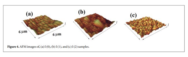
برای بررسی نوع فاز نمونه های رسوب شده، سیستم پراش سنج پراش اشعه ایکس (XRD) فیلیپ X’Pert-MPD با تابش Cu-Kα مورد استفاده قرار گرفته است. تجزیه و تحلیل عنصری توسط یک میکروسکوپ الکترونی اسکن انتشار میدانی TE-SCAN (FESEM) با پیوست یک تجزیه کننده اشعه ایکس پراکنده انرژی (EDX) حاصل شد. توپوگرافی نمونه های رسوب شده توسط میکروسکوپ نیروی اتمی (AFM- ARA AFM) کنترل شد. APHILIPS CM120TEM برای مطالعه شکل و اندازه ذرات SnS استفاده شد. فوتولومینسانس دمای اتاق واریان كاری اکلیپس (PL) برای تجزیه و تحلیل خواص نوری نمونه های نانوساختار SnS استفاده شد.
Abstract
An electrochemical route has been employed to prepare pure SnS and indium-doped SnS thin films. Six samples including undoped SnS and In-doped SnS thin films deposited on the fluorine-doped tin oxide (FTO) glass substrates. An aqueous solution having SnCl2 and Na2S2O3 used as the primary electrolyte. Different In-doped SnS samples were prepared by adding a different amount of 1 mM InCl3 solution into the first electrolyte. The applied potential (E), time of deposition (t), pH and bath temperature (T)were kept at −1 V, 30 min, 2.1 and 60 °C, respectively. For all samples, except the Indopant concentration, all the deposition parameters are the same. After preparation, X-ray diffraction (XRD), field emission scanning electron microscopy (FESEM)with an energy dispersive X-ray analyzer(EDX) attachment, atomic force microscopy (AFM), and transmission electron microscopy (TEM)were used to determine structural properties of as-deposited films. XRD patterns revealed that the synthesized undoped- and In-doped SnS thin films were crystallized in the orthorhombic structure. The shape of SnS crystals was spherical in the TEM image. X-ray peak broadening studies was done by applying Scherrer’s method, Williamson-Hall (W–H) models(including uniform deformation model (UDM), uniform strain deformation model (UDSM), and uniform deformation energy density model (UDEDM)), and size-strain plot (SSP) method. Using these techniques, the crystallite size and the lattice strains have been predicted. There was a good agreement in the particle size achieved by W–H- and SSP methods with TEM image.
1. Introduction
In recent years, tin sulfide (SnS) has attracted much attention, with an extensive range of applications such as in near-infrared detectors, electrochemical capacitors[1], holographic recording, photovoltaic cells, and lithiumion batteries, [2–8]. SnS is a semiconductor belongs to the IV–VI group, which it has a long b-axis with lattice constants of a = 0.4321 nm, b = 1.119 23 nm, and c = 0.398 38 nm [9]. It has a layered structure. According to figure 1, SnS consists of two weakly van der Waals force bonded layers, in which atoms are tightly bonded with covalence bond. SnS has a variety of energy band gap which related to the preparation method. The band gap of SnS has been reported as 1.3–2.3 eV for direct band gap and 1.0–1.2 eV for indirect band gap [10]. Because of the unique features of SnS such as high absorption coefficient(>104 cm−1 ) [11], suitable carrier concentration [9], plentiful in nature, non-toxicity, and cost efficiency, it was a promising candidate for use in absorber layers in thin film solar cell applications.
Various techniques were used to deposit SnS such as spray pyrolytic-deposition [12–14], molecular beam epitaxy (MBE)[15], hydrothermal method [6, 7, 16], chemical bath deposition [17–20], electron beam evaporation [21, 22], SILAR method [23], and electrodeposition technique [11, 24]. The electrochemical route is a good method due to simplicity, cost-efficiency, and the facility of controlling its parameters with high accuracy. Also, this method is inexpensive [25].
To estimate the crystallite size of material, the Scherrer’s method has been applied. Nevertheless, two essential factors including inhomogeneous strain and instrumental effects have not taken into account for acquiring crystallite size. Therefore, the W–H and SSP methods are an average technique to a much realistic estimation of the crystallite size and lattice strain [26]. As we know, the diffraction peaks will be broadened due to the deviation from perfect crystallinity. From peak width analysis, it can be obtained the crystallite size and lattice strain. The particle size is almost bigger than crystallite size due to the aggregation of crystallite structures [27]. In order to a real crystal deviate from a perfect crystal, the lattice strain has been created. The sources of lattice strain are crystalline defects such as dislocations, grain boundaries, triple junctions, sinter stresses, stacking faults, coherency stresses, etc. Some structural parameters such as the breath of peaks, the peaks intensity and the peak position shifts impacted on crystallite size and lattice strain. The peak width and the lattice strain depended on the 1/cos θ and tan θ, respectively [28]. In order to obtain the crystallite size and lattice strain as a function of 2 θ, it can be used by two methods named Williamson-Hall (W–H)- and the size-strain plot(SSP) methods.
In this work, six samples(containing undoped SnS and In-doped SnS) have been synthesized by electrochemical deposition from an aqueous solution. With the use of XRD data, the crystallite size, the lattice strain, and the other associated parameters have been achieved by UDM, UDSM, UDEDM, and the SSP methods. The crystallite size values acquired from Scherrer’s method, W–H, and SSP methods confirmed by TEM image. We found that the W–H and SSP methods have not yet been investigated on the In-doped SnS thin films.
2. Experimental
2.1. Materials and processing
Pure and In-doped SnS thin films deposited using an electrochemical route on fluorine-doped tin oxide (FTO) coated glass substrate. The effective surface area of FTO substrates(used as working electrode)was 1 cm × 1 cm. A platinum sheet and a saturated calomel electrode (SCE)were used as the anode and the reference electrode, respectively. The electrolyte was an aqueous solution of SnCl2 (2 mM) and Na2S2O3 (16 mM), and InCl3 (1 mM) aqueous solution supplied the In-dopant. By adding diluted H2SO4, the pH of solution reduced from 3.8 to 2.1. Before the deposition process, the FTO and the platinum sheet cleaned and then rinsed with ethanol/acetone and distilled water. The temperature of the bath was 60 °C. The deposition process was done during 30 min. In addition, by a computer-controlled electrochemical analyzer(potentiostat, Autolab, A3ut71167, Netherlands), the applied deposition potential kept constant at −1 V. After the deposition process, the substrates were taken out from the bath and washed with distilled water. Following relation shows the mechanism of the formation of SnS on cathode electrode,
According to the above reactions, the Na2S2O3 is unstable in acidic media. Therefore, it is easy to separate the sulfur, and consequently, the Sn2+ and S reduced at the cathode (substrate) to form SnS. In this study, pure SnS and In-doped SnS thin films were prepared using electrodeposition method. The undoped SnS named as I(0), and the In-doped SnS thin films named as I(1)–I(5). Using EDX analysis, the atomic percentage of In-dopant in I(1), I(2), I(3), I(4), and I(5)samples obtained 1.30, 2.13, 2.59, 2.90, and 3.58%, respectively.
2.2. Characterization of the films
In order to inspect the type of phases of the deposited samples, a Philips X’Pert-MPD x-ray diffraction diffractometer(XRD)system with Cu-Kα radiation has been employed. Elemental analysis was achieved by a TE-SCAN field emission scanning electron microscopy (FESEM)with an energy dispersive X-ray analyzer (EDX) attachment. The topography of the deposited samples checked by atomic force microscopy (AFM- ARA AFM). A PHILIPS CM120 TEM was used to study the shape and the size of SnS particles. Varian-Cary Eclipse room temperature photoluminescence (PL)was employed to analyze the optical characterization of nanostructured SnS samples.
چکیده
1. مقدمه
2. تجربی
2.1 مواد و فرایند
2.2 ویژگی لایه ها
3. نتایج و بحث
3.1 تجزیه و تحلیل XRD
3.2 اندازه و فشار کریستالیت
3.3. PL
3.4. خواص الکتریکی
4. نتیجه گیری
Abstract
1. Introduction
2. Experimental
2.1. Materials and processing
2.2. Characterization of the films
3. Results and discussion
3.1. XRD analysis
3.2. Crystallite size and strain
3.3. PL
3.4. Electrical properties
4. Conclusion
References