
دانلود رایگان مقاله حسگرهای مبتنی بر گرافن، دیگر مواد دو بعدی و سیستم های ترکیبی
گرافن و بقیه مواد دو بعدی، مانند فلز گذار dichalcogenide، به سرعت به عنوان بلوکهای ساختاری جذاب برای کاربردهای اپتوالکترونیک، همراه با تمرکز قوی روی پلتفرمهای مختلف تشخیص نور، خود را به اثبات رساندهاند. تطبیقپذیری این سیستمهای مواد، کاربرد آنها را در نواحی شامل تشخیص بسیار سریع و با حساسیت بالای نور در رنج فرکانسی ماوراء بنفش، نور مرئی، مادون قرمز و تراهرتز، امکانپذیر میکند. این حسگرها همانند تکنولوژیهای الکترونیک و فوتونیک سیلیکون، میتوانند با دیگر اجزای فوتونیک مبتنی بر همان مواد، در کنار یکدیگر قرار گیرند. در اینجا، حسگرهای نوری مبتنی بر گرافن مدرن، سایر مواد دوبعدی و سیستمهای هیبرید مبتنی بر ترکیب بلورهای دو بعدی مختلف یا بلورهای دو بعدی و دیگر مواد (نانو)، مانند نانوذرات پلاسماسون، نیمه هادی ها، نقاط کوانتومی یا ادغام آنها با موجکهای سیلیکون را مرور و ارزیابی میکنیم.
تبدیل نور به سیگنالهای الکتریکی در صدر تکنولوژی قرار دارد دهد. کاربردهای شامل تصویربرداری ویدئویی، ارتباطات نوری، تصویربرداری بیومدیکال، امنیت، دید در شب، حسگر گاز و تشخیص حرکت، به دلیل توسعه مواد با کارایی بالا و تکنولوژی تولید و یکپارچهسازی در مقیاس بزرگ به سطح بالایی از پیشرفت رسیده است. با وجود رشد مقیاس و تنوع نواحی کاربردی، نیاز به یک پلتفرم تشخیص نور با کارایی بالاتر در زمینه سرعت، کارایی یا رنج طول موج، به اندازه انعطافپذیری، شفافیت و اجتماعپذیری CMOS، روز به روز برجستهتر میشود.
گرافن ماده جذابی برای فوتونیک و اپتوالکترونیک است زیرا در مقایسه با مواد دیگر مزایای متعددی ارائه می دهد. انواع دستگاه های اپتوالکترونیک نمونه اولیه ، مانند الکترودهای شفاف در نمایشگرها و ماژول های فتوولتائیک، مدولاتورهای نوری ، دستگاه های پلاسمونی و لیزرهای فوق سریع، تاکنون نشان داده شده است. در بین اینها، بیشترین تلاش برای پیشرفت سنسورهای نوری، براساس تعدادی از ویژگی های متمایز گرافن و مواد مرتبط (GRM)، صورت گرفته است. اول، گرافن بدون شکاف است. این ویژگی منحصربفرد، تولید حاملهای بار از طریق جذب نور را در طیف بسیار وسیعی از انرژی، امکانپذیر میکند. این رنج وسیع اشعه ماوراء بنفش، نورمرئی، مادون قرمز موج کوتاه (SWIR)، نزدیک مادون قرمز (NIR)، میان مادون قرمز (MIR)، مادون قرمز دور (FIR) و رگرسیون طیفی تراهرتز (THz) را در برمیگیرد. همچنین، گرافن دارای دینامیک حامل بار بسیار سریع، جذب مستقل طول موج، خواص نوری قابل تنظیم از طریق دوپینگ الکترواستاتیک، نرخ تخلیه کم و تحرک بالا و توانایی محدود کردن انرژی الکترومغناطیسی به حجم بیسابقه کم است. تحرکپذیری بسیار بالای حاملها باعث تبدیل سریع فوتون و یا پلاسمون به جریان الکتریکی یا ولتاژ می شود.
بسیاری از این ویژگیها و قابلیتهای منحصربفرد سیستمهای تشخیص نور مبتنی بر گرافن، در طول چند سال اخیر مطالعه شده و به کاربردهای مختلفی اشاره شده است. بعضی از این ویژگیها در حال حاضر با رقابت با تکنولوژی های موجود به رقابت های تجاری دست پیدا کرده اند. از همه مهمتر، گرافن با پلتفرم مبتنی بر سیلیکون بسیار پیشرفته برای الکترونیک و فوتونیک سازگار بوده، و آن را به عنوان یک رقیب قوی برای ادغام هزینه کم و مقیاس بزرگ در شبکه های اپتوالکترونیک و مدارهای خواندن چند پیکسلی CMOS سازگار قرار میدهد.
گرافن تنها یکی از تعداد زیادی از بلورهای دو بعدی (2D) است که در حال حاضر تنها شروع به بررسی میشوند. صدها مواد لایه ای وجود دارد که ثبات آنها را تا به تک لایه ها حفظ می کند و خواص آنها مکمل گرافن است. اکسید فلزی گذرا (TMOs) و فلز گذرای dichalcogenides (TMDs) دارای ساختار لایه ای هستند. اتمهای هر لایه توسط پیوند کووالانسی کنار یکدیگر نگه داشته میشوند، در حالی که لایههای مختلف توسط نیروی واندروالانسی در کنار یکدیگر قرار میگیرند. در مقایسه با نیمههادیهای با شکاف باند مستقیم کلاسیک، TDMها به دلیل شفافیت، انعطافپذیری مکانیکی و پردازش آسان، مزایای اضافی را در زمینه اپتوالکترونیک ارائه میدهد. همچنین، تونایی تنظیم شکاف باند توسط تغییر تعداد لایهها (N)، تشخیص نور را در طول موجهای مختلف امکانپذیر میکند. این ویژگی ها از بسیاری جهات گرافن را تکمیل می کند: گرافن برای فناوری های باند پهن و فناوریهای سریع مفید است، در حالیکه TMD های نیمه هادی برای کاربردهایی که به جذب نور قوی و الکترولیومینسانس نیاز دارند، مفید هستند. یک رویکرد امیدوارکننده ترکیب این خواص و ایجاد دستگاههای هیبریدی و موادی چند منظوره و با کارایی بالا، شامل گرافن و سایر پشته های ناهمگن کریستال 2بعدی است. لایه های گرافن می توانند به عنوان الکترود قابل تنظیم به کار برده شوند، در حالیکه TMD ها به عنوان مواد عکس برداری فعال استفاده می شوند، که نشاندهنده تعامل قوی نور و جذب فوتون هستند.
در این بررسی، ما در مورد وضعیت فعلی مدرن تشخیص نور بر اساس GRM ها و سیستم های ترکیبیای بحث میکنیم که بوسیله ترکیبی از کریستال های دوبعدی مختلف یا کریستال های 2بعدی و دیگر مواد (نانو) مانند نانوذرات پلاسمونی، نقاط کوانتومی، یا توسط ترکیب GRMها با موجکهای سیلیکونی، ایجاد شدهاند. در ابتدا، اصطلاحات و مکانیسم های فیزیکی پایهای تشخیص تشخیص نور ، و سپس تجربیات آزمایشی انواع مختلفی از دستگاههای حسگر نور، از جمله تکنیک های افزایش حساسیت و جذب نور مورد بحث قرار گرفته است. با بحث در مورد سطوح پیشرفت و عملکرد سیستم های پیشرفته تشخیص نور GRM، در مقایسه با تکنولوژی های موجود نتیجهگیری میکنیم.
مکانیزمهای فیزیکی قادر به تشخیص نور
اصل کلیدی که تشخیص فوتوژن و دیگر کاربردهای اپتوالکترونیک به آن متکی هستند، تبدیل فوتونهای جذب شده به سیگنال الکتریکی است. چندین مکانیزم متفاوت در گرافن که توسط آن این تبدیل صورت میگیرد، گزارش شدهاست. این روشها شامل تاثیر فتوولتائیک، تاثیر ترموالکتریک نوری، اثر بالومتریک، اثر فوتوگیتینگ و مکانیزمی که از موج پلاسما کمک میگیرد میباشد. در ادامه، ما این مکانیزم ها، که در چه زمانی هر یک از آنها برجسته شده و اهمیت آنها در تشخیص نور مبتنی بر GRM را توصیف میکنیم.
توجه شود که اصطلاحات مربوطه، واحدها و عناصر کلیدی شایستگیها برای حسگر نور (مانند مفاهیم جریان نور، سرعت، راندمان کوانتومی داخلی و خارجی، حساسیت، تشخیص، قدرت برابر با نویز و افزایش هدایت فوتونی) در جعبه 1 خلاصه شده است.
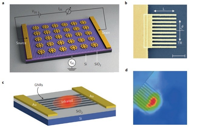
اثر فتوولتائیک. تولید جریان نور فوتوولتائیک (PV) براساس جداسازی جفت الکترون-حفره (e-h) تولیدشده با نور بوده که توسط میدان های الکتریکی موجود در اتصالات بین نواحی آلاییده شده مثبت (p-type) و منفی (n-type) گرافن یا بین بخشهای با آلایش متفاوت، ایجاد میشود. همان اثر را می توان با استفاده از ولتاژ بایاس سورس-درین(Vbias)، ایجاد کرد که یک میدان الکتریکی خارجی تولید میکند. اما این به طور کلی در مورد گرافن اجتناب می شود، چون یک نیمه رسانا است و بنابراین یک جریان تاریک بزرگ تولید می کند. میدان ساخته شده را می توان نتیجه دوپینگ شیمیایی در محل دانست که به صورت الکترواستاتیکی با استفاده از گیتها یا با استفاده از تفاوت عملکرد بین گرافن و یک فلز متصل ایجاد میشود. در مورد گیتهای تقسیم شده، دوپینگ می تواند بسته به ولتاژهای اعمال شده به گیت، به صورت p یا n تنظیم شود، در حالیکه در مورد اتصالات گرافن و فلز، دوپینگ در ناحیه تماس ثابت می شود. به طور معمول برای فلزات با عملکرد کاری بالاتر از گرافن ذاتی (4.45 eV) p-type است، در حالی که کانال گرافن می تواند p یا n باشد. جهت جریان نور فقط به جهت میدان الکتریکی بستگی دارد، و نه به سطح دوپینگ. بنابراين، هنگاميکه از p-n به n-p يا از +p-p به p-p+، میرود، تغییر علامت میدهد، که p + به معناي دوپينگ p-type قوی تر نسبت به p است.
یادآور میشویم که پراکندگی الکترون-الکترون (e-e) می تواند به تبدیل یک جفت الکترون-حفره با انرژی بالا به جفت های چندگانه e-h با انرژی پایین تر منجر شود. این فرایند، همچنین به عنوان ضرب حامل شناخته می شود، که به طور بالقوه می تواند کارایی کلی تشخیص نور را افزایش دهد.
Graphene and other two-dimensional materials, such as transition metal dichalcogenides, have rapidly established themselves as intriguing building blocks for optoelectronic applications, with a strong focus on various photodetection platforms. The versatility of these material systems enables their application in areas including ultrafast and ultrasensitive detection of light in the ultraviolet, visible, infrared and terahertz frequency ranges. These detectors can be integrated with other photonic components based on the same material, as well as with silicon photonic and electronic technologies. Here, we provide an overview and evaluation of state-of-the-art photodetectors based on graphene, other two-dimensional materials, and hybrid systems based on the combination of different two-dimensional crystals or of two-dimensional crystals and other (nano)materials, such as plasmonic nanoparticles, semiconductors, quantum dots, or their integration with (silicon) waveguides.
The conversion of light into electrical signals is at the heart of a multitude of technologies that affect our daily lives. Applications, including video imaging, optical communications, biomedical imaging, security, night-vision, gas sensing and motion detection have reached a high level of maturity due to the development of highperformance materials and large-scale production and integration technologies. Although the scale and diversity of application areas are growing, the need for a photodetection platform with higher performance in terms of speed, efficiency or wavelength range, as well as flexibility, transparency and complementary metal–oxide–semiconductor (CMOS) integrability, is becoming more eminent.
Graphene is an appealing material for photonics and optoelectronics because it offers several advantages compared with other materials1–5. A variety of prototype optoelectronic devices have already been demonstrated, such as transparent electrodes in displays6 and photovoltaic modules7,8, optical modulators9 , plasmonic devices10 and ultrafast lasers3 . Among these, significant effort has been devoted to developing photodetectors, based on a number of distinct characteristics of graphene and related materials (GRMs). First, graphene is gapless. This enables charge carrier generation by light absorption over a very wide energy spectrum, unmatched by any other material. This includes the ultraviolet, visible, short-wave infrared (SWIR), near-infrared (NIR), mid-infrared (MIR), farinfrared (FIR) and terahertz (THz) spectral regimes. Furthermore, graphene exhibits ultrafast carrier dynamics11,12, wavelength-independent absorption13–15, tunable optical properties via electrostatic doping16,17, low dissipation rates and high mobility, and the ability to confine electromagnetic energy to unprecedented small volumes4,5. The high carrier mobility enables ultrafast conversion of photons or plasmons to electrical currents or voltages18,19.
Many of the characteristics and unique capabilities of photodetection systems based on graphene have been studied over the past few years, and several applications have been addressed. Some of these have already reached a level of competitiveness with existing technologies that may spark interest for commercialization. Importantly, graphene is compatible with the highly mature silicon-based platform for electronics and photonics20–22, making it a strong contender for low-cost and large-scale integration into optoelectronic networks and multipixel CMOS read-out circuits.
Graphene is just one of a large number of possible two-dimenional (2D) crystals that are only now beginning to be investigated23,24. There are hundreds of layered materials that retain their stability down to monolayers, and whose properties are complementary to those of graphene. Transition metal oxides (TMOs) and transition metal dichalcogenides (TMDs) have a layered structure25. Atoms within each layer are held together by covalent bonds, while different layers are mainly held together by van der Waals interactions25. Compared with classical direct-bandgap semiconductors, TMDs can offer additional advantages in the context of optoelectronics because of their transparency, mechanical flexibility and easy processing. Moreover, the ability to tune the bandgap by varying the number of layers (N) allows the detection of light at different wavelengths. These properties complement those of graphene in many ways: graphene is useful for broadband, ultrafast technologies, whereas semiconducting TMDs are advantageous for applications requiring strong light absorption and electroluminescence. A promising approach is to combine these properties and create multifunctional, high-performance materials consisting of graphene and other 2D crystal heterogeneous stacks and hybrid devices. Graphene layers can be employed as work-function tunable electrodes, while TMDs are utilized as photoactive material, displaying strong light–matter interaction and photon absorption.
In this Review, we discuss the current state-of-the-art of photodetectors based on GRMs and hybrid systems realized by the combination of different 2D crystals or of 2D crystals and other (nano) materials, such as plasmonic nanoparticles, quantum dots (QDs), or by the integration of GRMs with silicon waveguides. First, the terminology and basic physical mechanisms of photodetection are discussed, then the experimental realizations of various kinds of photodetector, including techniques to enhance sensitivities and light absorption. We conclude with a critical discussion on the level of maturity and performance of current state-of-the-art GRM photodetection platforms in comparison with existing technologies.
Physical mechanisms enabling photodetection
The key principle on which photodetection and other optoelectronic applications rely is the conversion of absorbed photons into an electrical signal. Several different mechanisms by which this can be accomplished in graphene have been reported. These include the photovoltaic effect, the photo-thermoelectric effect, the bolometric effect, the photogating effect and the plasma-wave-assisted mechanism. In the following, we describe these mechanisms, when each of them may become dominant and their manifestations in GRM-based photodetectors.
Note that the relevant terminology, units and key figures of merits for photodetectors (such as the concepts of photocurrent, speed, internal and external quantum efficiencies, responsivity, detectivity, noise-equivalent power and photoconductive gain) are summarized in Box 1.
Photovoltaic effect. Photovoltaic (PV) photocurrent generation is based on the separation of photogenerated electron–hole (e–h) pairs by built-in electric fields at junctions between positively (p-type) and negatively (n-type) doped regions of graphene or between differently doped sections26–28 (Fig. 1b,d). The same effect can be achieved by applying a source–drain bias voltage (Vbias), producing an external electric field. But this is generally avoided in the case of graphene, as it is a semimetal and therefore it generates a large dark current. The built-in field can be introduced either by local chemical doping29, electrostatically by the use of (split) gates26,30, or by taking advantage of the work-function difference between graphene and a contacting metal26–28,31. In the case of split gates, the doping can be tuned to be p or n, depending on the applied gate voltages, whereas in the case of graphene–metal junctions the doping in the contacted area is fixed. This is typically p-type for metals with a work function higher than that of intrinsic graphene (4.45 eV), whereas the graphene channel can be p or n. The photocurrent direction depends only on the direction of the electric field, not on the overall doping level. Thus, it switches sign when going from p–n to n–p, or from p–p+ to p+–p, where p+ means stronger p-type doping compared with p.
We note that electron–electron (e–e) scattering32–34 can lead to the conversion of one high-energy e–h pair into multiple e–h pairs of lower energy12,33,35. This process, also denoted as carrier multiplication, can potentially enhance the overall photodetection efficiency.
مکانیزمهای فیزیکی قادر به تشخیص نور
دسته بندی حسگر های نور
زمینه های کاربردی، چالش ها و دیدگاه ها
Physical mechanisms enabling photodetection
Classes of photodetectors
Application fields, challenges and perspectives