
دانلود رایگان مقاله کالیبراسیون چند مرحله ای کاملاً قطعی مبتنی بر ADC برای ADC های خط لوله
خلاصه
کالیبراسیون پس زمینه دیجیتال به طور کامل قطعی برای ADC ها خط لوله ارائه شده است. روش پیشنهادی بر اساس مفهوم انشعابADC به کوتاه ترین زمان کالیبراسیون پس زمینه با دقت بالااست. روش میانگین شیب عدم تطابق در یک طرح کالیبراسیون چند مرحله ای استفاده شده است تا تشخیص خطاهای مدار بدون هر گونه عملیات تکراری و یا بازخورد حلقه ها انجام شود، که ارائه آن سریع و دقیق است. تجزیه و تحلیل رفتارشبیه سازی شده برای کالیبراسیون چند مرحله ای توسعه یافته کارایی این تکنیک و شایستگی خود را برتکنیک مبتنی برLMS نشان میدهد. ملاحظات عملی در نظر گرفته شده وکالیبراسیون ارائه شده بر روی یک CMOS 40 نانومتر 200Ms/sاعمال شده است. نتایج شبیه سازی شده چرخه کالیبراسیون بسیار سریع را نشان می دهد ، که در آن ADC به بیش از 11 ENOB در کمتر از 1600 چرخه کلاک رسیده است.
1. مقدمه
مبدل های آنالوگ به دیجیتال با کارایی بالانیازمندند که پردازش های دیجیتالی را برای ورودی RF در سیستم های ارتباطی پهن باند تا حد امکان فشرده کنند. این کارانعطاف پذیری بالاتر و سطح ادغام بالاتر باراندمان مصرف انرژی بهتر را قادر می سازد دارد[1].برای عملکردهایی با سرعت بالا و وضوح بالا،Pipeline ADC مناسب ترین معماری را ارائه می دهد که در شکل 1برای ADC 12بیتی نشان داده شده است.این یک چندی کننده (quantizer) دامنه چند مرحله ای است که دیجیتال کردن توسط خط لوله کردن تعدادی از از مراحل مشابه یا یکسان انکدرهای آنالوگ به دیجیتال کیفیت پایین انجام شده است که مبدل های پایه (sub-converter) آنالوگ به دیجیتال (ADSC) نامیده میشوند.خروجی ADSC هرمرحله خط لوله با سیگنال ورودی اش توسط مبدل آنالوگ به دیجیتال ضرب کننده(MDAC) پردازش شده است،که با مبدل انالوگ به دیجیتال پایه (ADSC) ترکیب شده،تفریق و تقویت در مدار خازن سوئیچ شده (SC) انجام می شود.دقت MDAC به بهره بالای تقویت کننده در سرعت مورد نیاز ADC بستگی دارد.طراحی سریع تقویت کننده با بهره بالا، با پیشرفت فن آوری پیچیده تر و توان نا کارامدتر می شود،که ویژگی طول ترانزیستور را برای سرعت های بالاترکاهش می دهد که در عملکرد آنالوگ کمتر و استفاده از ولتاژ کمتر هزینه بر است.
یک روش کارآمد برای قدرت نفوذ وضوح موثر آنالوگ در سرعت بالا استفاده از تقویت کننده ها با بهره پایین است که برای درجه بندی صحیح برای رفع محدودیت مدار آنالوگ استفاده می شود[2]. این روش به خوبی با روند تکنولوژی که در آن پردازش دیجیتال در حال سریعتر شدن و کارایی توان بیشتر است، مطابقت دارد.درجه بندی دیجیتال را می توان با ایجاد وقفه در عملکرد طبیعی ADC در پیش زمینه،یا می توان با اجرا تبدیل نرمال ADC در طول پس زمینه، انجام داد.درجه بندی پس زمینه عملکردADC بدون درز و انحراف کارایی مسیرها در سراسر تغییرات دما را ضمانت می کند،که ارائه درجه بندی قوی و موثر است. در میان تکنیک های درجه بندی پس زمینه های مختلف، درجه بندی ADC دو بخش شده است یکی که در [3] معرفی شده ودیگری به عنوان تکامل یک روش قطعی و عملی برای درجه بندی ADCها با سرعت بالاست. بر خلاف روش های دیگر [4] - [6]، درجه بندی ADC محدوده دینامیکی سیگنال ورودی را حفظ می کند، سنجش و تصحیح خطارا فراهم می کند، و چرخه کالیبراسیون در یک زمان بسیار کمتر و انجام می شود.یک روش جالب از ADC دو بخشی در [7] ارائه شده است که درجه بندی خطاهای MDAC را به سرعت انجام می دهد. این روش در [8] بیشتر توسعه یافته ، که درجه بندی سریع تر و دقیق تری را با استفاده از میانگین عدم تطابق شیب (SMA) به منظور تصحیح بهره محدود تقویت کننده ها و نمونه برداری خازن عدم تطابق را می دهد.
این کار با هدف گسترش روش SMA در ADCدو بخشی برای کالیبراسیون چند مرحله ای و با توجه به محدودیت های عملی آن با تجزیه و تحلیل، در یک Pipeline ADC 40 نانومتری شبیه سازی و استفاده شده است.بخش دوم یک بررسی اجمالی از ADC دو بخشی انجام می دهد.بخش سوم بحث و تجزیه و تحلیل از درجه بندی دیجیتال قطعی ADC دو بخشی را ارائه می دهد.بخش چهارم توسعه طرح درجه بندی پس زمینه را معرفی می کند.بخش پنجم ملاحظات عملی روش ارائه شده را می دهد و در نهایت بخش ششم از نتایج بدست آمده نتیجه گیری می کند.
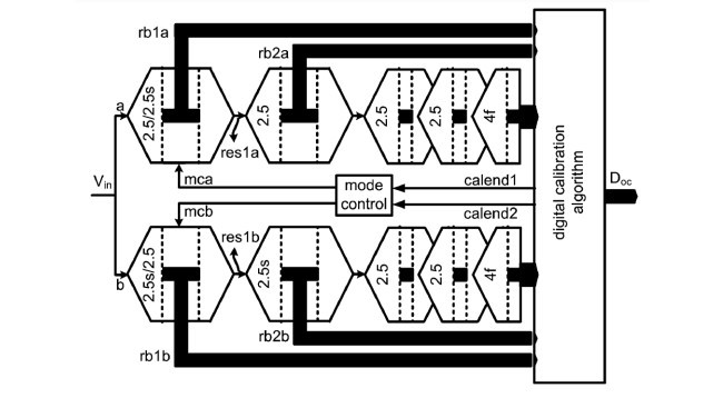
2. درجه بندی ADC دو بخشی : مفهوم و بررسی اجمالی
درجه بندی ADC دو بخشی یک مرجع را برای تشخیص خطا با تقسیم ADC تک کانال به دو نیمه فراهم میکند همانطور که در شکل 2 نشان داده شده است. هر یک از دو نیمه از نیمی از خازن های نمونه برداری Cs و نیمی از تقویت هدایت انتقالی gm، ADC تک کانال اصلی استفاده می کند،بنابراین ADC دو بخشی نزدیک به همان توان و ناحیه را حفظ میکند.سپس درجه بندی پس زمینه در ناحیه دیجیتال با استفاده از خروجی کانال های هر دو ADC دو بخشی Doa و Dob انجام شده است.تفاوت بین خروجی های دو کانال برای تشخیص خطا استفاده می شود،که بلوک های تصحیح خطا را برای هر کانال ADC با پارامتر های تصحیح مربوطه تغذیه می کند.خروجی های درجه بندی شده هر دو کانال Doac و Dobc هستند که برای بازیابی خروجی درجه بندی نهایی ADC Doc میانگین گیری شده اند.
در [9] و [10]، روش های کالیبراسیون ADC دو بخشی غیر قطعی با حالت های باقی مانده های متعدد در مرحله درجه بندی ADC دو بخشی به منظورارائه یک تشخیص خطا قوی استفاده شده است. حالت باقی مانده متعدد استفاده شده در این روش حاکی از استفاده بهره پایین در مرحله Pipeline به منظور محاسبه برای استانه افست های مقایسه کننده بیش از محدوده است.مرحله بهره پایین به این معنی است که نیاز به توسعه دقت ADC در بیشتر مراحل لازم خواهد شد.هم چنین تصحیح با به روز کردن پارامترهای درجه بندی از میان حلقه انطباقی با استفاده از LMS (الگوریتم حداقل متوسط مربع) انجام شده است،که ضرورت زمان اضافی برای همگرایی حلقه است. در [7]، درجه بندی ADC دوبخشی برای یک Pipeline ADC با تغییر ویژگی های باقی مانده از هر درجه بندی نیمه ADCدوبخشی با توجه به یکی دیگردر نظر گرفته شده است ، و برآورد مستقیم خطا برای بهره محدودتقویت کننده و عدم تطابق خازن با در نظر گرفتن تفاوت دو خروجی کانال تقسیم انجام شده است. با این حال، به منظور انجام این کار، یک حلقه LMS برای اصلاح عدم تطابق خطای بهره بین دو ADC تقسیم شده استفاده شده است که روی دقت برآورد خطا و افزایش زمان درجه بندی تاثیر میگذارد. حلقه LMS باید درنرخ بسیار کندتر از الگوریتم کالیبراسیون برای عملکرد صحیح همگراباشد، که در هنگام استفاده از این روش محدودیت اضافه می کند. همچنیناین روش در [7] ارائه شده است که برای درجه بندی چند مرحله ای مناسب نیست ، که به از استفاده از رزولوشن بالاتردر مرحله اول برای کاهش خطاهای ورودی از باطن تنظیم نشده ADC (BE ADC)اشاره دارد . استفاده از رزولوشن بالاتر مرحله Pipeline حداکثر سرعت مبدل را محدود می کند و احتیاج دقیقی به افست های مقایسه کننده ADSC دارد.
3. درجه بندی ADC دو بخشی چند مرحله ای: عملکرد و تحلیل و بررسی
کاهش محدودیت های قبلی کار ADCدوبخشی در بخش دوم اشاره شد، ما توسعه روش (SMA)به درجه بندی چند مرحله ای ارائه می دهیم. با تجزیه و تحلیل عملکرد ADCدو بخشی برای چند مرحله ای، یک رویکرد کاملا قطعی در نظر گرفته شده است. این رویکرد قطعی بدان معنی است که تشخیص خطاو اصلاح بدون هیچ گونه تقریب محاسبات و یا تخمین انجام شده است، و در نتیجه باعث می شود درجه بندی بسیاردقیق و سریع شود، بسته به سطح نویزADC و پردازش دیجیتال بهینه سازی لازم است. تجزیه و تحلیل ونتیجه گیری آن در این بخش ارائه شده است، و به دنبال آن دربخش های زیر طرح درجه بندی چند مرحله ای پیشنهادشده مورد بحث است.
تشخیص خطا مدار در Pipeline ADC دوبخشی می تواند بطورمستقیم با استفاده ازانتقال باقی مانده در مرحله درجه بندی انجام شود[7]. این خطای مدار، که دلیل آن بهره محدود تقویت کننده وعدم تطابق خازن است، به نظر می رسد که در آستانه تصمیم گیری هرباقی مانده در آن مراجع کم و یا اضافه شده است.
Abstract
A fully deterministic digital background calibration for pipeline ADCs is presented. The proposed approach is based on split ADC concept to give the shortest background calibration time with high accuracy. A slope mismatch averaging technique is employed in a multistage calibration scheme to deterministically detect the circuit errors without any iterative operations or feedback loops, which render it fast and accurate. Analysis and behavioral simulations for the developed multistage calibration demonstrate the efficiency of this technique and its merit over the LMS-based techniques. Practical considerations have been considered and the proposed calibration has been applied on a 200 MS/s 40 nm CMOS split pipeline ADC to correct for the capacitor mismatch and the amplifier finite gain. The post-layout simulation results show a very fast calibration cycle, where the ADC achieves more than 11 ENOB in less than 1600 clock cycles.
I. INTRODUCTION
HIGH performance analog-to-digital converters are needed to push the digital processing as close as possible to the RF input in wideband communication systems. This enables higher flexibility and higher integration level with better power efficiency [1]. For high resolution and high speed applications, the pipeline ADC represents the most suitable architecture, and it is shown in Fig. 1 for a 12-bit ADC. It is a multi-step amplitude quantizer in which digitization is performed by pipelining a number of similar or identical stages of low-resolution analog-to-digital encoders called the analog-to-digital sub-converter (ADSC). The ADSC output of each pipelined stage is processed with its input signal by the multiplying digital to analog converter (MDAC), which combines the digital-to-analog sub-converter (DASC), signal subtraction and amplification in a single switched capacitor (SC) circuit. The precision of the MDAC depends on a high gain amplifier at the ADC required speed. Designing a fast settling high gain amplifier is becoming more complex and power inefficient with the technology advances, which reduce the transistor feature length for higher speed on the expense of lower analog performance and use lower supply voltages.
An efficient method to leverage the effective analog resolution at high speed using low gain amplifiers is to use digital calibration to correct for the analog circuit limitations [2]. This method conforms well with technology trend in which digita processing is becoming faster and more power efficient. Digital calibration can be done by interrupting the ADC normal operation in the foreground, or it can be run in the background during the normal conversion of the ADC. Background calibration ensures a seamless ADC operation and tracks performance deviation across temperature variations, which render the calibration robust and effective. Among different background calibration techniques, split ADC calibration has been introduced in [3] and evolved as a promising and practical technique to calibrate high speed ADCs. Unlike other techniques [4]–[6], split ADC calibration preserves the dynamic range of the input signal, provides robust error measurement and correction, and performs the calibration cycle in a much less time. An interesting split ADC technique is presented in [7], which performs a rapid calibration of MDAC errors. This technique is further developed in [8], which gives more accurate and faster calibration using slope mismatch averaging (SMA) to correct for amplifier finite gain and sampling capacitor mismatch.
This work aims at extending the SMA technique in split ADC for multistage calibration, and considering its practical limits by analysis, simulations and applying it on a 40 nm pipeline ADC. Section II presents an overview on the split ADC calibration. Section III discusses and analyses the split ADC deterministic digital calibration. Section IV introduces the developed background calibration scheme. Section V presents the practical considerations of the proposed technique and finally Section VI concludes the achieved results.
II. SPLIT ADC CALIBRATION: CONCEPT AND OVERVIEW
The split ADC calibration provides a reference for error detection by splitting the single channel ADC into two halves as shown in Fig. 2. Each one of the two halves uses half the sampling capacitances and half the amplifier transconductance of the original single channel ADC, thus the split ADC preserves nearly the same power and area. The background calibration is then performed in the digital domain using the digital outputs of both split ADC channels and . The difference between the two channel outputs is used for error detection which feeds the error correction block for each ADC channel with the corresponding correction parameters. The calibrated outputs of both channels and are then averaged to recover the final calibrated output of the ADC .
In [9] and [10], non-deterministic split ADC calibration approaches are used with multiple residue modes in the calibrated split ADC stage to provide a robust error detection. The multiple residue modes used in these techniques imply the use of lower gain in the pipelined stage to account for over-range due to comparator threshold offsets. This lower gain stage means that more stages will be needed to provide the required ADC accuracy. Also, the correction is performed by updating certain calibration parameters through an adaptive loop using LMS (Least Mean Square algorithm), which necessitates extra time for loop convergence. In [7], the split ADC calibration is considered for a pipeline ADC by shifting the residue characteristics of each calibrated split ADC half with respect to the other one, and direct error estimation for finite amplifier gain and capacitor mismatch is done by taking the difference of the two split channel outputs. However, in order to do this, a LMS loop has been used to correct the gain error mismatch between the two split ADC halves, which affects the accuracy of error estimation and increases the calibration time. The LMS loop should converge at a much slower rate than the calibration algorithm for correct operation, which adds constraints when using this technique. Also this technique as presented in [7] is not suitable for multistage calibration, which implies the use of higher resolution first stage to decrease the input-referred errors of the uncalibrated backend ADC (BE ADC). The use of higher resolution pipelined stage limits the maximum speed of the converter and puts stringent requirement on the comparator offsets of the ADSC.
III. MULTISTAGE SPLIT ADC CALIBRATION: OPERATION AND ANALYSIS
To alleviate the limitations of previous split ADC work mentioned in Section II, we propose the extension of (SMA) technique to multistage calibration. By analyzing the split ADC operation for multistage, a fully deterministic approach has been considered. This deterministic approach means that the error detection and correction have been done without any approximate calculations or estimators, and thus makes the calibration very accurate and fast, depending on the ADC noise-level and digital post-processing optimization requirements. The analysis and its conclusion is presented in this section, and the following section will discuss the proposed multistage calibration scheme.
Circuit error detection in split pipeline ADC can be performed directly by using shifted residues in the calibrated stage [7]. This circuit error, which is caused by amplifier finite gain and capacitor mismatch, appears at the decision thresholds of each residue where the references are subtracted or added.
خلاصه
1. مقدمه
2. درجه بندی ADC دو بخشی : مفهوم و بررسی اجمالی
3. درجه بندی ADC دو بخشی چند مرحله ای: عملکرد و تحلیل و بررسی
4. درجه بندی کاملا قطعی ADC دو بخشی
A. شیب متوسط عدم تطابق
B. درجه چند مرحله ای بندی قطعی
C. روش درجه بندی پس زمینه
5. ملاحظات عملی و نتایج شبیه سازی شده
A. تاثیر نویز و دقت درجه بندی
B.تاثیرویژگی های سیگنال ورودی بر درجه بندی پس زمینه
C.کاربرد Pipeline Split ADC در CMOS 40 نانومتری
D. ناحیه و توان بالای تقسیم ADC
6. نتیجه
منابع
Abstract
1. INTRODUCTION
2. SPLIT ADC CALIBRATION: CONCEPT AND OVERVIEW
3. MULTISTAGE SPLIT ADC CALIBRATION: OPERATION AND ANALYSIS
4. FULLY DETERMINISTIC SPLIT ADC CALIBRATION
A. Slope Mismatch Averaging
B. Deterministic Multistage Calibration
C. Background Calibration Procedure
5. PRACTICAL CONSIDERATIONS AND SIMULATION RESULTS
A. Noise Effect on Calibration Accuracy
B. Effect of Input Signal Characteristics on the Background Calibration
C. Application on Split Pipeline ADC in 40 nm CMOS
D. Area and Power Overhead of Splitting the ADC
6. CONCLUSION
REFERENCES