
دانلود رایگان مقاله روش لوله کشی برای طراحی ADC SAR کم مصرف و سرعت بالا
چکیده
در این مقاله یک مبدل آنالوگ به دیجیتال با توان پایین (ADC) ارائه شده است که براساس روش راه اندازی خط لوله بکار رفته در معماری SAR (رجیستر تقریب متوالی) می باشد. این ساختار یک SAR ADC خط لوله دو مرحله ای می باشد که دارای کانال های نامتقارن TI (جاداده شده در زمان) می باشد، که هدف آن دستیابی به نرخ بالای نمونه برداری تا حدود سه برابر یک SAR ADC معمولی می باشد، و در عین حال دارای مزیت مصرف توان پایین و ناحیه کوچک باشد. به منظور طراحی یک مبدل دقیق، سرعت بالا و با توان پایین، از تبدیل منفعل باقیمانده بدون استفاده از آمپلی فایر میانی و مشارکت سمفونیک مراحل استفاده شده است. در معماری پیشنهادی، در طول فرآیند تبدیل، هر نمونه سیگنال تجربه ای مشابه آفست مقایسه کننده دارد، که دلیل آن به خاطر عملیات جدیدی است که اعمال شده است، بدون آنکه شماتیک چرخش مقایسه کننده یا حالت افزونگی اضافه گردد. براساس معماری پیشنهادی، یک ADC هفت بیتی با نرخ نمونه برداری 83 MS/s طراحی شده است و عملکرد آن با نتایج شبیه سازی طرح قبلی در یک تکنولوژی 180-nm CMOSمورد بررسی قرار گرفته است.تحلیل سطح سیستم و تائیدیه های شبیه سازی هردو نشان دهنده برتری معماری پیشنهادی نسبت به دیگر معماری های مشابه SAR می باشند.
1. مقدمه
مبدل آنالوگ به دیجیتال (ADC) یکی از بلاک های کلیدی سیستم های سیگنال ترکیبی می باشد. این مبدل بایستی با توجه مصرف توان و عملکرد، به صورت بهینه طراحی شود. به منظور برآوردن الزامات مختلف از جمله سرعت بالا، مصرف توان و رزولوشن، معماری های مختلف ADC مثل خط لوله، فلش، فولدینگ و رجیستر تقریب متوالی (SAR) ارائه شده است. SAR ADC به عنوان یک معماری سرعت بالا، توان پایین و با پیچیدگی کم شناخته شده است، زیرا برای تعیین N بیت ورودی آنالوگ، در طول N سیکل ساعت تنها از یک مبدل استفاده می کند{1،2}. این ویژگی موجب می شود تا SAR ADC تبدیل به یکی از معروفترین معماری ها برای برنامه های بیسیم، پزشکی و برنامه های مدرن سیار تبدیل شود. علاوه بر این، مقیاس بندی CMOS موجب افزایش نرخ نمونه برداری و کاهش مصرف توان SAR ADC ها شده است، که در اینجا ADC های لوله گذاری شده جایگزین شده است و دلیل آن به خاطر پهنای باند بیشتر سیگنال ورودی می باشد{3،4}.
به منظور دستیابی به عملکرد موردنظر ADC، تحقیقات معمولاً بروی ارتقا تکنیک های مدار و یا ارائه معماری های جدید تمرکز دارند. مزایای SAR ADC موجب شده است که به گزینه جذابی برای ارائه معماری های ترکیبی جدید تبدیل شود{5-18}. این معماری ها برای افزایش نرخ نمونه برداری و یا رزولوشن SAR ADC از تکنیک های مختلفی استفاده می کنند، و در عین حال از مزیت مصرف توان نیز بهره مند می باشند. ADC های IT و لوله گذاری شده مبتنی بر SAR، متداول ترین معماری می باشند که توسط بیشتر تکنیک های سیستماتیک ارتقا یافته، پشتیبانی می شوند.
یک SAR لوله گذاری شده معمولی، در میان تمامی مراحل از یک مبدل MDAC (دیجیتال به آنالوگ) با آمپلی فایر باقیمانده استفاده می کند{5،6}. به منظور ارائه ADC هایی با سرعت و رزولوشن بالا، بایستی MDAC بهره بالا طراحی گردد؛ اگرچه این مسئله موجب افزایش مصرف توان برای پهنای باند وسیع ورودی می گردد و با پایین آمدن مقیاس تکنولوژی، مشکل تر می شود که دلیل آن کاهش بهره ترانزیستورها و کاهش ولتاژ تغذیه می باشد. به منظور غلبه بر این مشکلات، برخی از ساختارهای SAR لوله گذاری شده سعی کرده اند MDAC را جایگزین و یا حذف نمایند، و یا آن را به اشتراک بگذارند{7-12}. به اشتراک گذاری یک MDAC منحصربفرد میان تمامی مراحل، موجب ارتقا بهره وری انرژی می گردد؛ اگرچه با توجه به بکارگیری یک MDAC در مراحل مختلف، ممکن است یکسری خطای بهره بوجود آید،همچنین ممکن است محدودیت شدیدی بروی زمان مجاز برای تقویت باقیمانده بوجود آید. برای رفع این محدودیت، تکنیک های مختلفی برای ماکزیمم نمودن سرعت ADC پیاده سازی شده، ارائه شده است{7-9}، اما آنها توان بیشتری مصرف می کنند. جایگزین نمودن MDAC با یک مدار ساده bucket-brigade موجب کاهش مصرف توان می گردد، در این مدار برای دستیابی به بهره ولتاژ، شارژ از یک خازن بزرگتر به یک خازن کوچکتر منتقل می شود {10-11}. اما این مسئله موجب نشست نادرست و همچنین خطاهای غیرخطی و خطی دمای متغیر و سیگنال وابسته می گردد{11}. روش دیگر لوله گذاری در توپولوژی SAR، انتقال باقیمانده به صورت منفعل از مرحله اول به مرحله دوم می باشد، که بدین ترتیب مصرف توان آمپلی فایرهای میانی از بین می رود {12}. در این روش، شارژ باقیمانده ذخیره شده در خازن های مرحله اول، به مرحله دوم انتقال می یابد (با انتقال بخشی از مهمترین خازن (MSB) به مرحله دوم). مقایسه کننده ها نیز در میان تمامی مراحل انتقال می یابند، تا حالت غیرخطی کاهش یابد، و علت آن آفست نامساوی مقایسه کننده ها در مراحل مختلف می باشد{12}. عیب این معماری، کاهش دقت است که دلیل آن انتقال خازن مرحله اول (که نگهدارنده باقیمانده می باشد) به مرحله دوم می باشد. در این تقل و انتقال، شارژ باقیمانده ممکن است با بیش از یک LSB تغییر یابد، که دلیل آن به خاطر معایب مدار از جمله اشتراک گذاری شارژ و ایده آل نبودن سوئیچ ها می باشد. علاوه بر این، چرخش مقایسه کننده موجب افزایش قابل توجه سوئیچینگ می شود.
در TI SAR ADC ها، مصرف توان به صورت خطی و با تعداد کانال های IT افزایش می یابد ودقت به خاطر عدم تطابق میان کانال ها (مثل آفست، خطای بهره، و انحراف زمانبندی) کاهش می یابد. بنابراین، در این معماری ها نیاز به کالیبراسیون می باشد{13}. برای مینیمم نمودن مصرف توان در TI SAR ها، از تکنیک های مختلف مدار یا سیستم استفاده می گردد{14-17}. به طور مثال، لوله گذاری یک Flash ADC (به عنوان مرحله اول) و یک TI از SAR ADC (به عنوان مرحله دوم)، موجب کاهش تعداد سیکل های تبدیل می گردد و MDAC را حذف می کند{17}. اگرچه این توپولوژی از مزیت عملیات ذخیره و ردیابی ذاتی (T/H) بهره مند نمی باشد، که دلیل آن ADC فلش بکاررفته در مرحله اول می باشد و در ADC نهایی، نیاز به یک مدار T/H مجزا دارید. مدار اضافی T/H، ناحیه بسیار زیادی اشغال می کند و همچنین برای انجام عملیات، نیاز به یک شماتیک ساعت اضافی دارد{17،18}. علاوه بر این، افزایش تعداد بیت های موجود از توپولوژی فلش موجب افزایش تعداد مقایسه گرها می شود و این مسئله منجر به افزایش توان و کاهش حالت خطی می گردد{18}.
این مقاله یک روش لوله گذاری برای ارتقا عملکرد SAR ADC ارائه می کند، و در عین حال سعی دارد تا بهره وری انرژی را حفظ کند. ADC یک SAR لوله گذاری شده دو مرحله ای می باشد که دارای یم روش TI نامتقارن می باشد، این روش TI بروی هریک از مراحل اعمال شده است تا بدین ترتیب بتواند نرخ نمونه برداری را افزایش دهد. معماری SAR پیشنهادی از مزیت تبدیل باقیمانده منفعل بدون آمپلی فایر میانی بهره مند می باشد. ترتیب بهینه ای از مراحل عملیات و کانال ها ارائه شده است که موجب کاهش ناحیه، ارتقا بهره وری انرژی، و افزایش سرعت نمونه برداری در مقایسه با تحقیقات قبلی می گردد. این مزایا با توجه به تلاش های صورت گرفته در این تحقیق بدست آمده اند تا بدین ترتیب تعداد مقایسه کننده ها به حداقل برسد، آمپلی فایر میانی حذف گردد، تاثیر خازن ورودی مقایسه کننده ها کاهش یابد، تاثیر سوئیچ ها کاهش یابد، و در نهایت تعداد کانال های TI به حداقل برسد. رزولوشن و ظرفیت خازنی هر دو مرحله به گونه ای تنظیم شده است که میزان ظرفیت خازنی مرحله اول به حداقل می رسد و زمان نشست هر دو مرحله متعادل شده است. در روش پیشنهادی برعکس مقاله {12}، خازنی که نگهدارنده باقیمانده می باشد، میان مراحل حرکت نمی کند، در نتیجه باقیمانده تحت تاثیر معایب مدار قرار نمی گیرد. در عوض، از یک آرایه خازنی کمکی استفاده شده است که به پورت بیکار مقایسه کننده متصل شده است. علاوه بر این در مدار پیشنهادی، از شماتیک چرخش مقایسه کننده با عملیات سوئیچینگ زیاد استفاده نشده است، اگرچه سیگنال ها همان تجربه آفست مقایسه کننده در هر مقایسه را دارند.
مابقی مقاله به صورت زیر بخش بندی شده است: بخش 2 به معماری پیشنهادی ADC و جزئیات عملیاتش می پردازد. مقایسه سیستماتیک توپولوژی پیشنهادی SAR ADC با برخی دیگر از ساختارهای ADC در بخش 3 ارائه شده اند. بخش 4 به تحلیل خطی معماری پیشنهادی و طراحی آن می پردازد. بخش 5 به طراحی مدار میپردازد و در ادامه در بخش 6 به نتایج شبیه سازی طرح می پردازیم و در نهایت در بخش 7 به نتیجه گیری مقاله می پردازیم.
2. معماری ADC پیشنهادی
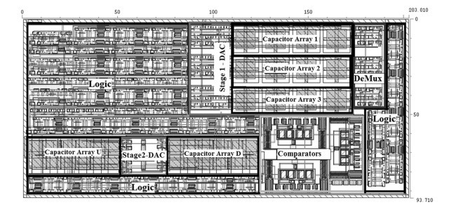
ADC یک SAR لوله گذاری شده دومرحله ای می باشد و دارای روش TI می باشد که بروی هر مرحله اعمال شده است. N1 مهمترین بیت ها MSBها (و N2 کم ارزشترین بیت ها (LSBها) برای N = N1 + N2 تبدیل بیت، به ترتیب توسط مرحله اول و دوم تولید شده اند. ADC شامل دو مرحله می باشد: یک کنترلر اصلی، و یک ژنراتور ولتاژ مرجع و یک الحاق کننده بیت. مرحله اول دارای سه کانال با نام های Ch1، Ch2 و Ch3 می باشد (همانطور که در شکل 1 مشاهده می کنید)، که هر یک شامل یک آرایه خازن بیت N1، یک منطق SAR، یک مالتی پلیکسر آنالوگ، و یک دی مالتی پلیکسر آنالوگ می باشد. مرحله دوم دارای دو کانال با نام های ChUp و ChDown می باشد (شکل 1)، که هر یک شامل یک آرایه خازن N2 بیت، یک منطق SAR، و یک دی مالتی پلیکسر آنالوگ می باشد. کانال های مرحله دارای هیچ مقایسه کننده ای نمی باشند. در طول مقایسات مختلف، آنها از مقایسه کننده های مرحله اول استفاده می کنند. دی مالتی پلیکسرهای آنالوگ مرحله دوم Analog Demux U (D) نام دارند (شکل 1)، و خروجی هریک از آرایه های خازن مرحله دوم را به مقایسه کننده ای از مرحله اول متصل می کنند (در طول تولید LSB توسط مرحله دوم). مالتی پلکیرها و دی مالتی پلیکسرهای آنالوگ مرحله اول (Analog Demux1 (2or3 و Analog Mux1 (2or3)) برای تکمیل این اتصال مورداستفاده قرار می گیرند. Analog Demux، خروجی هریک از مقایسه کننده ها را به منطق SAR مناسبی متصل می کند، و Analog Mux ولتاژ حالت معمول (Vcm) و یا خروجی آرایه خازن کانال های مرحله دوم را به مقایسه کننده متصل می کند. کنترلر اصلی در شکل 1، ترتیب عملیات هریک از بلاک های SAR را سازماندهی می کند و سیگنال های مورد نیاز را برای دی مالتی پلکسرهای آنالوگ ارائه می کند.
Abstract
A low power analog to digital converter (ADC), based on a pipelining method employed in successive approximation register (SAR) architecture is presented. This structure is a two-stage pipeline SAR ADC with asymmetrical time interleaved (TI) channels, aimed to reach sampling rate as high as about threefold of a conventional SAR ADC while benefiting from its low power consumption and small area. Passive residue conversion without inter-stage amplifier and symphonic collaboration of stages are employed to design a low power, high speed, and accurate converter. In the proposed architecture, every signal sample experiences equal comparator offset during its conversion due to the applied novel operation sequence, without adding redundancy or comparator rotation scheme. A 7-bit ADC with sampling rate of 83 MS/s based on the proposed architecture is designed and its performance is verified by post layout simulation results in a 180-nm CMOS Technology. Both system level analysis and simulation verifications support proposed architecture superiority over similar reported SAR architectures.
1 Introduction
Analog to digital converter (ADC) is one of the key functional blocks of any mixed signal system. It should be optimally designed concerning both performance and power consumption. Various ADC architectures such as pipeline, flash, folding and successive approximation register (SAR) have been employed to meet different requirements of sampling speed, power consumption and resolution. SAR ADC is known as a low-power, low-speed and low-complexity architecture, as it employs only a comparator over N clock cycles to determine N bits of the sampled analog input [1, 2]. This feature makes SAR ADC one of the most popular architectures for biomedical, modern portable and wireless applications. In addition, scaling of CMOS technology increases the sampling rate and reduces power consumption of SAR ADCs which are replacing pipelined ADCs due to their wider input signal bandwidth [3, 4].
To achieve the desired ADC performance, efforts are usually focused on improvement of circuit techniques or introduction of novel architectures. Advantages of the SAR ADC have made it attractive for introducing novel combinational architectures [5–18]. These architectures employ different techniques to increase sampling rate or resolution of SAR ADC while benefiting from its low power consumption. Pipelined and time interleaved (TI) ADCs based on SAR, supported by many improving systematic techniques, are the most common architectures.
A conventional pipelined SAR employs a multiplying digital-to-analog converter (MDAC) with a residue amplifier between stages [5, 6]. Designing high gain MDAC is needed for high resolution and high speed ADCs; however, it increases power consumption for wide input bandwidth and becomes more difficult as technology scales down due to the lower intrinsic gain of transistors and lower supply voltages. To overcome these issues, some reported pipelined SAR structures have tried to share, replace or omit the inter-stage MDAC [7–12]. Sharing a unique MDAC between stages improves power efficiency; however due to the use of a single MDAC in different stages, there are probable gain errors and also a rigid limitation on allowed time for residue amplification. To overcome this limitation, different timing-derived techniques have been employed to maximize the speed of implemented ADC [7–9], but they consumes extra power. Replacing MDAC with a simple bucket-brigade circuit, in which charge is moved from a large capacitor to a small capacitor to realize voltage gain, reduces power consumption especially in its Op-Amp-less realization [10, 11]; but it results in inaccurate settling besides signal dependent and temperature-variant linear and nonlinear errors [11]. Another method of pipelining in SAR topology is transferring the residue from the first stage to the second stage in a passive way to eliminate the power consumption of inter-stage amplifiers [12]. In this method, the residue charge stored on the first stage capacitors is transferred to the second stage by moving a part of the most significant bit (MSB) capacitor to the second stage. The comparators are also moved among stages to reduce the nonlinearity due to the unequal offset of comparators in different stages [12]. The disadvantage of this architecture is accuracy degradation due to the moving the first stage capacitor, which holds the residue, to the second stage. In this moving, the residue charge may be changed by more than one LSB because of circuit imperfections such as charge sharing and non-idealities of the switches. In addition, the employed comparator rotation increases the switching activity significantly.
In TI SAR ADCs, power consumption is increased linearly with the number of interleaved channels and accuracy degrades due to the mismatches between the channels, such as offset, gain error and timing skew. Therefore, calibration is necessary in these architectures [13]. Various circuit or system techniques have been utilized to minimize power consumption in TI SARs [14–17]. For example, pipelining a Flash ADC, as the first stage, and a TI of SAR ADCs, as the second stage, reduces the number of conversion cycles and eliminates the MDAC [17]. However, this topology does not benefit from the intrinsic track and hold (T/H) operation implemented in the SAR topology, due to the employed flash ADC in the first stage and a separate T/H circuit is required in the ADC front-end. The extra T/H circuit consumes excessive area and also requires an additional clock scheme for its operation [17, 18]. In addition, increasing available number of bits from the flash topology to raise the sampling rate increases the number of comparators and results in power increment and linearity degradation [18].
This paper presents a pipelining method for enhancing throughput of the SAR ADC while trying to retain its power efficiency. The ADC is a two stage pipelined SAR with an asymmetrical TI method applied to each stage for increasing the sampling rate. The proposed SAR architecture benefits from passive residue conversion without interstage amplifier. Optimal arrangement of operating stages and channels is proposed to reduce area, enhance power efficiency and increase sampling speed compared to the previous works. These advantages are achieved due to the attempts made in this work to minimize the number of comparators, eliminate the inter-stage amplifier, reduce the effect of comparators’ input parasitic capacitance, reduce the effect of switches and minimize the number of TI channels. Resolutions and hence the capacitance of the two stages are adjusted to minimize the amount of first stage capacitance and balance settling time of the two stages. In contrast to [12], the capacitor holding the residue is not moved between stages in the proposed method, so the residue is not impacted by circuit imperfections. Instead, an auxiliary capacitive array is employed and connected to the idle port of the comparator for residue conversion. In addition, the comparator rotation scheme with high switching activity, as used in [12], is not utilized in the proposed circuit, however, the signal experiences the same comparator offset in every comparison.
The rest of the paper is organized as follows: Sect. 2 explains the proposed ADC architecture and its operation details. Systematic comparison of the proposed SAR ADC topology with some other ADC structures is presented in Sect. 3. Section 4 covers linearity analysis of the proposed architecture and its design considerations. Section 5 describes circuit design, followed by post-layout simulation results in Sect. 6 and conclusions in Sect. 7.
2 Proposed ADC architecture
Figure 1 shows the overall architecture of the proposed ADC. The ADC is a two-stage pipelined SAR with TI method applied to each stage. N1 most significant bits (MSBs) and N2 least significant bits (LSBs) for N = N1 ? N2 bits conversion are produced by the first and the second stage, respectively. The ADC consists of two stages, a main controller, a reference voltage generator and a bit concatenator. The 1st-stage has three channels, named ‘‘Ch1, Ch2, and Ch3’’ in Fig. 1, each consists of an N1 bit capacitor array, a SAR logic, an analog multiplexer, and an analog de-multiplexer. The 2nd-stage has two channels, named ‘‘ChUp and ChDown’’ in Fig. 1, each consists of an N2 bit capacitor array, a SAR logic, and an analog de-multiplexer. The channels of the stage have no comparators. They employ each of the first stage comparators in different conversion intervals. The analog demultiplexers of the 2nd-stage, named ‘‘Analog Demux U (D)’’ in Fig. 1, connects the output of each capacitor array of the 2nd-stage to the appropriate comparator of the 1ststage during the LSB generation by the second stage. Analog multiplexers and de-multiplexers of the 1st-stage, named ‘‘Analog Demux1 (2or3)’’ and ‘‘Analog Mux1 (2or3)’’, are employed for completing this connection. Analog Demux connects output of each comparator to the appropriate SAR logic and Analog Mux connects the common mode voltage (Vcm) or output of the capacitor array of the 2nd-stage channels to the comparator. The main controller in Fig. 1 organizes the operation sequence of each SAR block and provides the required selection signals for the analog de-multiplexers.
چکیده
1. مقدمه
2. معماری ADC پیشنهادی
3. مقایسه سیستماتیک
4. ملاحظات طراحی و تلورانس حالت غیر ایده آل
5. پیاده سازی مدار
5.1 مقایسه کننده ها
5.2 آرایه های خازنی
5.3 منطق های SAR
5.4 کنترلر
6. نتایج شبیه سازی پیش طرح
منابع
Abstract
1 Introduction
2 Proposed ADC architecture
3 Systematic comparison
4 Design considerations and non-ideality tolerance
5 Circuit implementation
5.1 Comparators
5.2 Capacitor arrays
5.3 SAR logics
5.4 Controller
6 Post layout simulation results
References