
دانلود رایگان مقاله طراحی و توصیف مشخصات یک مبدل آنالوگ به دیجیتال فلش سه بیتی Gs/s-24
چکیده
این مقاله طراحی و توصیف مشخصات یک مبدل آنالوگ به دیجیتال فلش تک هسته ای سه بیتی Gs/s-24 در CMOS دیجیتال توان پایین 28 نانومتری ارائه میدهد.این مقاله مطالعه طراحی مدار نمونه بردار و نگهدار و مرحله بافر بعدی و محاسبات و معادلات برای پهنای باند را بدون شبیه سازی وسیع مدار ارائه می دهد. این نتایج با هدف کارایی سرعت لبه در یک ADC تک هسته ای استفاده شده اند.ADC قادربه دستیابی به نرخ نمونه برداری کامل بدون زمان جایگذاری است، که آن را سریع ترین ADC تک هسته ای در CMOS گزارش داده شده میسازد.بامصرف توان 0.4W وتعداد بیت موثر 2.2در Gs/s-24،ADC در حالیکه ناحیه فعال اشغال شده اش 12 mm2 به رقم شایستگی 3Pj در هر مرحله تبدیل می رسد. با توجه به فرکانس نمونه برداری بالا،این ADC هنگامی که با زمان متوسط جایگذاری بیت ترکیب ترکیب شود،قادر است که به سیستم مبدل آنالوگ به دیجیتال با سرعت فوق العاده بالا تبدیل شود.
1. مقدمه
سیستم های ارتباطی مدرن به نرخ داده تا چند ده گیگا بایت احتیاج دارند.یکی از چالش های ویژه ارتباط بی سیم board-to-board در ابرکامپیوترها است،که درآن توان داده بالای 100GS/s نیازاست. مشخصات فنی این را می توان با فرکانسهای حامل بالای100 گیگاهرتز به دست آورد،در این مورد پهنای باند بزرگ تا دهها گیگاهرتز در دسترس است.[1] سیستم ها باچنین پهنای باند بزرگ برای گنجانیده شدن در مبدل های آنالوگ به دیجیتال بسیار چالش آفرین هستند ((ADCs ، که به راحتی می تواند پیوندهای بیسیم تنگراه شوند.بعلاوه، یه منظور تهیه سیستم بر روی تراشه (SOCs)با پردازش سیگنال دیجیتال و ADC های مجتمع در همان تراشه، لازم است که ADC در تکنولوژی مدرن CMOS باشد. اخیرامبدل های آنالوگ به دیجیتال CMOS با بازده توان خوب با نرخ نمونه برداری در محدوده فرکانسی پایین تر [2],[5] با ثبت تقریبا متوالی نشان داده اند که ADC های محبوبی هستند. که رسیدن به بالاترین نرخ نمونه برداری با ساختار مدار پایه با بکار گیری جایگذازی زمانی ممکن است[8],[6].تازمانی که مولد کلاک چند فاز بالا ناچیز باشد،از لحاظ نظری افزایش نرخ نمونه برداری به اصطلاح بدون جریمه ضروری انرژی هر تبدیل ممکن است. به این دلیل توپولوژی های جایگذاری زمان استفاده شده برای ADC ها با سرعت بالا بسیاروسیع هستند و " بهره برداری گسترده ای به منظور رسیدن به رقم شایستگی پایین " داشته اند [9]، معادل انرژی کم در هر مرحله تبدیل در این زمینه.اخیرا نرخ نمونه برداری به بزرگی90Gs/s با هسته ADC ایی که درGs/s 14راه اندازی شده گزارش شده است.[10]متاسفانه استفاده از زمان جایگذاری در مقیاس دلخواه ممکن نیست،به عنوان مثال مشکلاتی سیستم جایگذاری شده رابه شدت محدود میکند، همانند مولد کلاک چند فاز و توزیع ، زمان انتقال کلاک، خازن های ورودی، احتیاج به تقویت کننده های نمونه بردار و نگهدار(THAs) ،و تاخیر[13]-[11],[9] . افزایش بیشترنرخ نمونه برداری بدون تشدید این مشکلات می تواند توسط پیاده سازی هسته سریع ترADCبدست آید.در حالیکه بالاترین ورودی پهنای باند در دسترس است این کاهش در مولد کلاک چند فاز و کاهش زمان تاخیر لازم است.
هدف طراحی برای ADC ارائه شده دستیابی به بالاترین سرعت نمونه برداری ممکن، در ADC تک هسته ای می باشد.درنتیجه توپولوژی فلش ADC انتخاب شده است.هسته ADC ارائه شده در حالیکه دریک CMOS دیجیتال کم توان و کم هزینه طراحی شده است،قادر به کارکردن در نرخ نمونه برداری تا 24Gs/s است. علاوه بر موضوعات مطرح شده در [14] ،این مقاله ملاحظات طراحی جامعی برای مراحل ورودی آنالوگ ارائه می دهد و بینشی از داخل تمامی بلوک های مدار ADC می دهد.علاوه بر این ،مقاله نتایج اندازه گیری شده اضافی و دقیق تر و همچنین فرکانس های بالای آماری را نشان می دهد.قسمت II معماری ADC را نشان می دهد. به عنوان پیاده سازی مدار برای چنین فرکانس های بالانیاز به ملاحظات طراحی جامع است، به ویژه برای مراحلی که ورودی آنالوگ دارند، مشخص کردن پهنای باند مورد نیاز برای بلوک های مدار بحرانی مهم است. بخش سوم به بررسی مدار نمونه بردار و نگهدار (T / H) و پس از آن مرحله بافررسیدگی میکند و یک روش محاسبه مستقیم پهنای باندمورد نیاز بدون شبیه سازی مدار گسترده را فراهم می کند.بینشی از داخل مدار اجرا شده در بخش IV داده شده در حالیکه در بخش V مشخصات تراشه ارائه شده است.
2. معماری ADC
شکل 1 نموداری از سطح سیستم ADC ارائه شده را نشان می دهد. برای بالاترین سرعت تبدیل، ADC متکی به توپولوژِی فلش است.این نمودار مرحله T/H و پس از آن بافر (Buf1) در ورودی،به دنبال آن یک مقایسه گر(Cmp)،بعلاوه تقویت کننده ها،و لچ ها (L) درهرمسیر موازی پردازش اطلاعات را نشان می دهد.سیگنال های خروجی باینری توسط تبدیل منطق دماسنجی به باینری (T2B) تولید شده اند.با استفاده ازفرآیند CMOS مدرن رسیدن به نرخ نمونه برداری ده ها گیگا هرتز با اندازه ساختار مدار در اندازه هزاران میکرومتر ممکن است.به دلیل اینکه دیگر اندازه مدار قابل اغماض نیست به طراحی RF از جمله شبیه سازی میدان مغناطیسی (EM) برای خطوط و سازه ها نیازاست.مراقبت ویژه ای برای گرفتن پهنای باند آنالوگ مواجه شده با بافر T/H و مقایسه گرها نیاز است. زمان هماهنگ سازی پس از مقایسه است که معمولا توسط یک فلیپ فلاپ اصلی-فرعی انجام می شود، که برای طراحی در فرکانس های ده ها گیگاهرتزبسیار چالش آفرین است. به منظور کاهش موثر زمان بازیابی، سه لچ و یک تقویت کننده در یک فلیپ فلاپ اصلی-فرعی-اصلی (MSM) ترکیب شده اند[15].
3. ملاحظات پهنای باند
نحوه عملکرد مدار در بالاترین سرعت نیاز به پهنای باند دقیق قابل توجه دارد.بیشترین نیاز درمرحله ورودی یک مدارT/H وپس از ان یک بافر است زیرا آنها در حوزه آنالوگ جایی که سیگنالها شامل زمان و اطلاعات دامنه می باشند کار می کنند.در حالیکه یک راه عمومی برای تعیین پهنای باند لازم توسط شبیه سازی ترانزیستور در حالت های پیچیده است ، این بخش معادلات کاربردی بر پایه مدل های ساده به منظور محاسبه پهنای باند هدف را ارائه می دهد.
.A مرحله TH
اساسی ترین توپولوژی یک خازن سوئیچ شده (SC)مدار T/H درشکل 2(b)نشان داده شده است.ترانزیستور M1 اتصال الکتریکی بین خروجی و ورودی مدار را کنترل می کند.در حالی که ورودی و خروجی در مرحله نگهداری فاز جدا شده اند و شارژ روی Ch حفظ شده است، اتصال الکتریکی در مرحله مسیر ایده آل باید یک اتصال کوتاه باشد.در این فاز امپدانس بین ورودی و خروجی به مقاومت درین-سورس M1 که بعنوان مقاومت Rt مدل شده است،بستگی دارد.
این باعث ایجاد یک فیلتر پایین گذر مرتبه اول بعنوان یک مدل ساده برای یک مدار SC T/H در حالت لبه می شود،همانطور که در شکل 2(b) نمایش داده شده است.برای فرکانس های ورودی نزدیک به فرکانس نایکوئیست ممکن است که دو ولتاژ متوالی نگهداشته شده در حداقل و حداکثر پوشش سیگنال ورودی باشند.در این مورد سیگنال خروجی مرحله T/H از مقدار حداقل تا حداکثر در یک دوره زمانی تغییرمی کند.این سناریو را می توان بایک مرحله از ورودی مرحله T/H با تقویت به مقدار peak-to-peak ولتاژ ورودی T/H مدل کرد.
B. بافرT/H
به غیر از طراحی مرحله H/ T پهنای باند بافر بعدی نیز مهم به نظرمی رسد.برای این بافر رسیدن به پهنای باند بالا مشکل است زیرا تمامی مقایسه کننده هایی را که یک بار خازنی بزرگ را به وجود آورده اند را راه اندازی می کند.از سوی دیگر این بافر بطور خاصی مهم است زیرا اگر پهنای باند خیلی کم شود ممکن است که وضوح موثرADC کاهش یابد،همانطور که در [16] توضیح داده شده است.در حالیکه در دیگر طراحی ها به طور تجربی به این نقطه بحرانی اشاره شده و فقط گاهی اوقات نتایج مشخصات پهنای باند داده شده[17]، این بخش یک روش به منظور محاسبه پهنای باند مورد نیاز را شرح می دهد که می تواند برای شرح خصوصیات سطح سیستم بدون شبیه سازی وسیع استفاده شود.
Abstract
This paper presents the design and characterization of a 24-GS/s 3-bit single-core flash analog-to-digital converter (ADC) in 28-nm low-power digital CMOS. It shows the design study of the track-and-hold circuit and subsequent buffer stage and provides equations for bandwidth calculations without extensive circuit simulations. These results are used to target leading-edge speed performance for a single ADC core. The ADC is capable of achieving its full sampling rate without time interleaving, which makes it the fastest single-core ADC in CMOS reported to date to the best of our knowledge. With a power consumption of 0.4 W and an effective number of bits of 2.2 at 24 GS/s, the ADC achieves a figure of merit of 3.6 pJ per conversion step while occupying an active area of 0.12 mm . Due to its high sampling frequency this ADC can enable ultra-high-speed ADC systems when combined with moderate time interleaving.
I. INTRODUCTION MODERN
communication systems require data rates up to several tens of Gb/s. One particularly challenging case is the wireless board-to-board communication in supercomputers, where data throughput above 100 Gb/s is needed. Technically this can be achieved with carrier frequencies above 100 GHz, as large bandwidths up to tens of GHz are available in this case [1]. Systems with such large bandwidth are very challenging for the incorporated analog-to-digital converters (ADCs), which can easily become the bottleneck of the wireless link. Additionally, in order to enable systems-on-chip (SOCs) with digital signal processing and ADCs integrated on the same chip, it becomes a requirement for the ADC to be realized in a modern CMOS technology. Recently published CMOS ADCs show good power efficiency at sampling rates in the lower GHz range [2]–[5] with successive approximation register (SAR) ADCs being most popular. It is possible to reach higher sampling rates with the same basic circuit structures by applying time interleaving [6]–[8]. As long as the overhead of multi-phase clock generation is negligible, it is theoretically possible to increase the sampling rate with no penalty in terms of required energy per conversion. For this reason time-interleaving topologies are widely used for high-speed ADCs and have been “extensively exploited to achieve low figures of merit” [9], equivalent to low energy per conversion step in this context. Recently, sampling rates as high as 90 GS/s have been reported with ADC cores running at 1.4 GS/s [10]. Unfortunately it is not possible to use time interleaving at an arbitrary scale, as several problems limit the performance of heavily interleaved systems, such as jitter in multi-phase clock generation and distribution, clock transition times, input capacitance, requirements on the track-and-hold amplifiers (THAs), and latency [9], [11]–[13]. Further increases in sampling rate without exacerbating those problems can be achieved by implementing faster ADC cores. This relaxes the requirements on the multi-phase clock generation and reduces the latency, while enabling highest input bandwidth.
The design goal for the presented ADC has been to achieve the highest possible sampling speed with a single ADC core. As a result, the flash ADC topology has been chosen. The presented ADC core is capable of working at sampling rates up to 24 GS/s , while being designed in a low-cost low-power digital CMOS technology. In addition to the topics presented in [14], this paper presents comprehensive design considerations for the analog input stages and gives insights into the circuit implementation of all ADC sub-blocks. Furthermore, it shows additional and more detailed measurement results, statically as well as at highest input frequencies. Section II shows the ADC architecture. As circuit implementations for such high frequencies require comprehensive design considerations, it is important to specify the bandwidth requirements for the critical circuit blocks, especially for the analog input stages. Section III investigates the track-and-hold (T/H) circuit and the subsequent buffer stage and provides a method to directly calculate the required bandwidth without extensive circuit simulations. Insights into the circuit implementation are given in Section IV, while Section V presents the chip characterization.
II. ADC ARCHITECTURE
Fig. 1 shows the system-level schematic of the presented ADC. For highest conversion speed, it relies on the flash topology. The schematic shows a T/H stage and subsequent buffer at the input, followed by a comparator (Cmp), further amplifiers, and latches (L) in each of the parallel data-processing paths. The binary output signals are generated by thermometer to binary conversion logic (T2B). By utilizing a modern CMOS process it is possible to achieve sampling rates of tens of GHz with circuit structure sizes in the range of hundreds of m. This requires RF design techniques including electromagnetic (EM) field simulations for lines and structures because the circuit size is no longer negligible. Special care needs to be taken of the bandwidth of the analog frontend consisting of the T/H buffer and the comparators. The time synchronization after the comparators is usually performed by a master–slave flip-flop, which is very challenging to design at frequencies of tens of GHz. In order to reduce the effective regeneration time, three latches and an amplifier have been combined to form a master–slave–master (MSM) flip-flop [15].
III. BANDWIDTH CONSIDERATIONS
Circuit operation at highest speed requires careful bandwidth consideration. The input stages consisting of a T/H circuit and subsequent buffer pose the highest requirements because they work in the analog domain where the signals contain time and amplitude information. While it is a common approach to determine the required bandwidth by complex transistor-level simulations, this section presents practical equations based on simple models to directly calculate the target bandwidth.
A. T/H Stage
The most basic topology of a switched capacitor (SC) T/H circuit is shown in Fig. 2(a). The transistor controls the electrical connection between the input and output of the circuit. While input and output are isolated during the hold phase and the charge on the hold capacitor is preserved, the electrical connection during the track phase should ideally be a short circuit. In this phase the impedance between input and output depends on the drain–source resistance of , which can be modeled as a resistor .
This creates a first-order low-pass filter as a simple model for a SC T/H circuit in track mode, as illustrated in Fig. 2(b). For input frequencies close to the Nyquist frequency it is possible that two consecutive hold voltages are at the minimum and at the maximum of the input signal envelope. In this case the output signal of the T/H stage has to change from the minimum value to the maximum within one tracking period. This scenario can be modeled with a step at the input of the T/H stage with the amplitude , the peak-to-peak value of the T/H input voltage. The corresponding step response converges exponentially towards the input step value with a time constant of , as shown in Fig. 3,
B. T/H Buffer
Apart from designing the T/H stage it is also important to consider the bandwidth of the subsequent buffer. High bandwidth is difficult to achieve for this buffer because it has to drive all comparators, which create a large capacitive load. On the other hand, this buffer is especially important because if its bandwidth is too low it will substantially decrease the effective ADC resolution, as has been described in [16]. While in other designs this critical point is addressed empirically and only sometimes the resulting bandwidth specifications are given [17], this section describes a method to calculate the bandwidth requirements for the T/H buffer, which can be used for system-level specifications without extensive circuit simulation.
چکیده
1. مقدمه
2. معماری ADC
3. ملاحظات پهنای باند
.A مرحله TH
B. بافرT/H
.4 پیاده سازی مدار
A. ملاحظات اساسی
B. مرحله T/H
C. بافرT/H
D. مقایسه کننده ها و جبران آفست
E. لچ ها
F. مولدکلاک
G. تبدیل منطقی کد دماسنجی به باینری
H. توزیع ولتاژ DC
I. ملاحظات طراحی
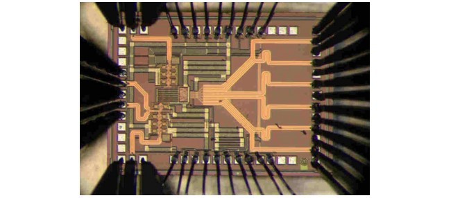
.5 اندازه گیری ها
A. راه اندازی اندازه گیری
B. نتایج تجربی
6. نتیجه گیری
منابع
Abstract
1. INTRODUCTION
2. ADC ARCHITECTURE
3. BANDWIDTH CONSIDERATIONS
A. T/H Stage
B. T/H Buffer
4. CIRCUIT IMPLEMENTATION
A. Basic Considerations
B. T/H Stage
C. T/H Buffer
D. Comparators and Offset Compensation
E. Latches
F. Clock Generation
G. Thermometer to Binary Conversion Logic
H. DC Voltage Distribution
I. Layout Considerations
5. MEASUREMENTS
A. Measurement Setup
B. Experimental Results
6. CONCLUSION
REFERENCES