
دانلود رایگان مقاله تاثیر مقیاس پذیری فناوری در کمبود قدرت سلول های استاندارد دیجیتال
چکیده
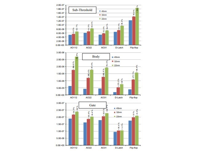
تخمین کمبود یک گام مهم در جریان طراحی دیجیتال با تکنولوژی نانو است. درحالیکه دادههای قابلاعتماد بر روند کمبود فنآوری CMOS در دستگاههای مستقل و مدارها وجود دارد، فقدان نتایج عمومی در اثر مقیاسپذیری در کمبود مصرف برق برای مجموعه استاندارد سلولی کامل است. تجزیهوتحلیلی بر روی کتابخانه سلول استاندارد بااستفاده از برآورد سطح منطق مدل، که توسط مقایسه SPICE BSIM 4پشتیبانی شده است ارائه میکنیم. افزایش سرعت مدل سطح منطق برروی SPICE 10^3< با متوسط دقت خطای زیر 1٪ است. بنابراین تاثیر مقیاسپذیری را در کل مجموعه سلولی استاندارد با توجه به مکانیزمهای مختلف کمبود (زیرآستانه، بدنه، گیت) بنا به وابستگی الگوی ورودی گسترش میدهیم. درحالیکه کمبود بدنه به نظر غالب میرسد، انتظار میرود کمبود زیرآستانه بیش از دیگر قطعات مقیاسپذیری افزایش یابد. اطلاعات دقیق از کل تجزیهوتحلیل برای استفاده در بیشتر تحقیقات در مورد طراحی دیجیتال گزارش شده است.
1. معرفی
بهطورکلی، اتلاف توان در مدارات دیجیتال میتواند در دو جزء مختلف گروهبندی شود:
1. قدرت پویا - ناشی از جریانهای مورد نیاز برای شارژ و تخلیه بار خازن در طول سوئیچینگ سیگنال و جریان اتصال کوتاه در معابر زمانی که هر دو بهطور همزمان به شبکه Pull-Up و PULL-DOWN میشوند.
2. قدرت استاتیک – زمانی رخ میدهد که حتی اگر هیچ انتقال سیگنالی با توجه به کمبود جریان در دستگاه وجود نداشته باشد.
کمبودجریان به شیوهای پیچیده بر روی خواص ساختار دستگاه مانند دوپینگ مشخصات، ضخامت اکسید، ابعاد کانال و غیره بستگی دارد، همانگونه که آنها به دلایل مختلف فیزیکی مانند گیت اکسید تونل، انتقال زیرآستانه و معکوس بایاس انتقال محل اتصال بستگی دارد. همانند استراتژی فناوری بین المللی برای نیمههادیها (ITRS) برای روند تلفات توان با توجه به پیشرفت تکنولوژی، تلفات استاتیک قدرت در CMOS نیز انتظار میرود که بیش از توان تلفات پویا باشد [5]. هانگونه که شکل. 1 نشان میدهد توان پویا منبع غالب اتلاف انرژی در سالهای گذشته بوده است، درحالحاضر قابلمقایسه است و حتی از کمبود زیرآستانه و کمبود اتصال پیشی گرفته است، درحالیکه کمبود اکسید گیت توسط معرفی دیالکتریک بالای K محدود شده است [5].
بهعنوان یک نتیجه، کمبود روشهای کاهش طراحی سطح مانند انتخاب الگوی ورودی [2]، تحویل و بایاس ولتاژ بدنه [7،9]، ترانزیستور خواب و آستانه دوتایی [15] ارائه شده است، همزمان برآورد فعلی کمبود، یک گام مهم و فزایندهای در طراحی جریان برای پیشبینی اثربخشی روش اعمال شده، همچنین بهدلیل وابستگی بسیار بالای کمبود جریان در تغییرات پارامتر تکنولوژی است [7،15].
مقیاسپذیری فنآوری، بنا به تقاضای بازار توابع بیشتری را در مدارات مجتمع میطلبد، به همین خاطر تعداد ترانزیستور و فرکانس عامل افزایش یافته است. بااینحال، مقیاسپذیری همواره موجب ترویج ناخواسته اتلاف انرژی به دلایلی مختلفی شده است. بهعنوان مثال، کوچکسازی طول کانال اثرات کانال را کاهش میدهد، که باعث افزایش زیرآستانه فعلی؛ مقیاسگذاری ضخامت جریان اکسید گیت و تاثیرگذاری در ولتاژ آستانه که در حال افزایش زیرآستانه است [19]. در نهایت، نه تنها ولتاژ حرارتی (KT / Q) بلکه سیلیکون نیز با مقیاسپذیری تغییر مییابد. ولتاژ ثابت حرارتی، در غیرمقیاسپذیری معکوس شیب ولتاژ زیرآستانه نتیجه شده است درحالیکه باند سیلیکون ثابت از شکاف درغیرمقیاسپذیری و در محل اتصال بالقوه و عرض لایه تخلیه ساخته شده است. بنابراین تراکم ترانزیستور، قابلیت و سرعت مقیاسپذیری تکنولوژی از یک سو افزایش یافت، قدرت تراکم و تنوع نیز از سوی دیگر [24] افزایش یافته است.
در چنین مواقعی، ارزیابی واضح تاثیر مقیاسپذیری بر رفتار قدرت کمبود و ترکیب، در یک کتابخانه سلولی کامل، نه در دستگاهها یا مدارهای جدا شده و ساده آزمون از منافع بزرگ است. برآورد زود هنگام و دقیق جریان کمبود در جریان طراحی برای در نظر گرفتن گرفتن اقدامات متقابل مبتنی بر فنآوری و مبتنی بر طراحی با ارزش است. برآورد جریان نشتی در سطح SPICE نتایج دقیق را تضمین میکند، اما برآورد جریان نشتی در مدارهای یکپارچه (IC) با پیچیدگی بالا/متوسط و حتی کمتر عملی نیست از زمانی که تکرار مونت کارلو برای تجزیهوتحلیل آماری اثرات تغییرات تکنولوژی بر نشت جریان مورد نیاز قرار گرفت. علاوه بر این، شبیهسازی سطح SPICE اجازه نمیدهد که یک تمایز ساده در میان کمکهای مختلف منابع فیزیکی نشت در یک IC پیچیده وجود داشته باشد، که یک تعریف روشنی از اقدام متقابل مبادلات است. ازسویدیگر، مدلهای برآورد سطح منطق را میتوان برای محاسبات سریعتر استفاده کرد. تلاشهای بسیاری در سال گذشته بهمنظور تعریف محاسبه قدرت نشت سریع در سطح منطق با دقت بالا انجام شده است، که میتواند قبل از اجرای مدار طراحی [10،13،1] به کار برده شود. تکنیک ارائه شده در [1] یک رویکرد در مدلسازی جریانهای نشتی در سطح منطق HDL ارائه میکند، که قادر است دقت بسیار خوبی بهدست آورد و بههمان اندازه برای فنآوریهای مقیاسپذیر معتبر است.
این کار، تجزیهوتحلیلی از جریانهای نشتی محاسبه شده برای یک کتابخانه سلول استاندارد کلی ارائه میکند هنگامیکه مقیاسپذیری تکنولوژی CMOS، تأییدی در سطح SPICE از نتایج بهدست آمده گزارش میکند. ما تاثیر جریانهای نشتی با فنآوریهای مقیاسپذیر از فنآوری 45 نانومتر به 32 نانومتر و 22 نانومتر (جدول 1) را تحلیل میکنیم.
با استفاده از قابلیتهای مدل موجود در [1]، تاثیر تکنولوژی مقیاسپذیری را بهطورجداگانه در سه جزء اصلی نشت بهعنوان مثال نشست Gate، نشت زیرآستانه و نشت اتصال، ازجمله الگوی ورودی وابستگی و اثرات انباشتگی تا سه انباشتگی MOSFET نشان میدهیم. بارگذاری اثر را نیز میتوان در فنآوری داده شده آزمایشهای ما گنجاند که تاثیر کلی آن نامرتبط است. مقاله به شرح زیر ساختاربندی شده است: در بخش 2، شش مدل فعلی نشت از تلفات توان از نظر مدل محاسبه سطح منطق توضیح و تفسیرشده است؛ بخش 3 مدل محاسبه نشت و پیادهسازی استفاده شده را مورد بحث قرار میدهد. بخش 4 گزارش نتایج نشت را از طریق SPICE و VHDL همراه با خطای بین آنها در سه فنآوری مقیاسپذیر برای همه الگوهای ورودی در 16 سلول استاندارد بیان میکند. بخش 5 به تجزیهوتحلیل وابسته به ترکیب ورودی از سه نشست بزرگ قطعات در سه فنآوری مقیاسپذیر برای 16 سلول اختصاص داده شده است، در بخش 6 نتیجهگیری بیان شده است.
Abstract
Leakage estimation is an important step in nano-scale technology digital design flows. While reliable data exist on leakage trends with bulk CMOS technology scaling in stand-alone devices and circuits, there is a lack of public domain results on the effect of scaling on leakage power consumption for a complete standard cell set. We present an analysis on a standard cell library applying a logic-level estimation model, supported by SPICE BSIM4 comparison. The logic-level model speedup over SPICE is 4103 with average accuracy below 1% error. We therefore explore the effects of scaling on the whole standard cell set with respect to different leakage mechanisms (sub-threshold, body, gate) and to input pattern dependence. While body leakage appears to be dominant, sub-threshold leakage is expected to increase more than other components with scaling. Detailed data of the whole analysis are reported for use in further research on leakage aware digital design.
1. Introduction
Broadly speaking, power dissipation in digital circuits can be grouped in two different components:
1. Dynamic power – resulting from the currents needed to charge and discharge load capacitances during signal switching and from short circuit current in transitions when both the pull-up and pull-down networks are simultaneously on.
2. Static power – occurring even if there is no signal transition, due to leakage currents in the devices.
Leakage currents depend in a complex manner on the device structure properties like doping profile, gate oxide thickness, channel dimensions etc., as they are due to different physical phenomena such as gate oxide tunneling, sub-threshold conduction and reverse bias junction conduction. As per International Technology Road-map for Semiconductors (ITRS) for the trend of power dissipation with respect to technology progress, static power dissipation in bulk CMOS is expected to exceed dynamic power dissipation [5]. Fig. 1 shows that while dynamic power was the dominant source of power dissipation in past years, now it is comparable or even surpassed by the sub-threshold leakage and junction leakage, while gate oxide leakage has been limited by the introduction high-K dielectrics [5].
As a consequence, design-level leakage reduction techniques have been proposed, such as input-pattern selection [2], supply and body voltage biasing [7,9], sleep transistors and dual threshold [15]; at the same time leakage current estimation is an increasingly critical step in the design flows for predicting the effectiveness of the applied technique, also because of the extremely high dependence of leakage currents on technology parameter variations [7,15].
Technology scaling, pushed by the market demand for more and more functions in ICs, has always been done for the sake of increasing transistor count and operating frequency. However, scaling always promotes unwanted leakage power dissipation for several reasons. As an example, downsizing of the channel length gives rise to short channel effects, which increases the sub-threshold current; scaling oxide thickness increases the gate tunneling currents and affects the threshold voltage which in turns increases sub-threshold current [19]. Ultimately, neither the thermal voltage (KT/q) nor the silicon band gap change with scaling. Constant thermal voltage results in non-scaling of the inverse sub-threshold voltage slope while constant silicon band gap results in non-scalability of built-in junction potential and depletion layer width. Therefore transistor density, functionality and speed have increased with technology scaling on one hand, but power density and variability have also increased on the other hand [24].
In such scenario, it is of great interest to have a clear assessment of the impact of scaling on leakage power behavior and composition, in a complete cell library rather than in single devices or isolated simple test circuits. An early and accurate estimation of the leakage currents in the design flow is valuable for considering technology-based and design-based countermeasures. Estimation of leakage currents at SPICE level guarantees the most accurate results, but it is not feasible means for estimating leakage currents in medium/high complexity integrated circuits (IC), and even less when Monte Carlo iterations are needed for the statistical analysis of technology variation effects on leakage currents. Moreover, SPICE-level simulation does not allow a straightforward distinction among the contributions of different physical sources of leakage in a complex IC, which would allow a more clear definition of countermeasure trade-offs. On the other hand, logic level estimation models can be used for its inherently faster computation. Many efforts have been done in the last years in order to define fast leakage power calculation at logic level with as high as possible accuracy, which could be applied before getting to the circuit implementation of the design [10,13,1]. The technique described in [1] presents an approach at logic level HDL modeling of leakage currents, which is capable of obtaining very good accuracy and is equally valid for scaled technologies.
This work presents an analysis of calculated leakage currents for a whole standard cell library when scaling bulk CMOS technology, reporting the verification at SPICE level of the obtained conclusions. We analyze the impact of leakage currents with technologies scaled from 45 nm technology to 32 nm and 22 nm (Table 1). By utilizing the capabilities of the model described in [1], we also show the impact of technology scaling separately on the three major leakage component i.e. gate leakage, sub-threshold leakage and junction leakage, including input pattern dependence and stacking effects up to three stacked MOSFETs. Loading effect can be also included, though in the given technologies our experiments showed that the overall impact is not relevant. The paper is organized as follows: in Section 2, six-leakage current model of static power dissipation is explained and interpreted in the view of the logic level calculation model; Section 3 discusses the leakage calculation model and the used implementation. Section 4 reports the leakage results through SPICE and VHDL along with error % between them in three scaled technologies for all input patterns in 16 standard cells, sub-categorized by their fan-in. Section 5 is devoted to the input combination dependent analysis of the three major leakage components in the three scaled technologies for the 16 cells, followed by Conclusions in Section 6.
چکیده
1. معرفی
2. بررسی مکانیسمهای نشت در فنآوریهای مقیاسپذیر
3. مدل محاسبه نشت
4. مقایسه جریان نشتی برآورد شده در فنآوری مقیاسپذیر
5. تجزیهوتحلیل موضوع اجزای نشت به اثرات مقیاسپذیری
6. نتیجهگیری
منابع
Abstract
1. Introduction
2. Review of leakage mechanisms in scaled technologies
3. Leakage calculation model
4. Comparison of estimated leakage currents in scaled technologies
5. Analysis of leakage components subject to scaling effects
6. Conclusions
References