
دانلود رایگان مقاله نانوسیم های GaP شکاف باند مستقیم پیش بینی شده
نانوسیم GaP یک ماده بالقوه برای دستگاه های جدید است که کاربردهای اپتیکال و الکترونیکی می توانند باهم ادغام شوند، از تعدادی از محدودیتها رنج می برد زیرا شکاف باند غیرمستقیم را نشان می دهد. با استفاده از محاسبات اولین اصول ما نشان می دهیم که به خاطر اثرات محدود کردن، شکاف باند نه تنها زمانیکه به شکل یک نانوسیم است بزرگ می شود ، بلکه می تواند تنها با کاهش چند نانومتری قطر نانوسیم به یک نانوسیم نیم رسانای شکاف باند مستقیم تبدیل شود. این تبدیل به یک شکاف باند مستقیم برای نانوسیم های GaP با جهت [111] روی دهد ولی نه برای نانوسیم های GaP با جهت [110]. اثرات وضعیتهای سطح که می تواند شکاف باند را تغییر دهد با اشباع هیدروژن و لایه سرپوش اکسید بر روی سطح نانومتر GaP مورد مطالعه قرار گرفته است. نتایج نشان می دهند در حالیکه هیدروژن یک غیرفعال کننده کامل است، پیوندناجور Ga2O3GaP/ پیوند باند رسانش کوچکی را نشان می دهد ولی نانوسیم های GaP با جهت [111] باند شکاف مستقیم را نگه می دارد.
1. مقدمه
نانوسیم های نیمه رسانای III-V به خاطر کاربرد باقوه شان در وسایل فتوالکترونیک و مدارهای فوتونی به شدت مورد مطالعه قرار گرفته اند. فسفیدگالیلوم تعداد زیادی از اشکال مقیاس نانوی مختلف را نشان می دهد، و در بین کاربردهای مختلفجالب می توان کاربرد آن برای دستگاههای ریز اپتیکال را نام برد. همچنانکه نانوسیم های فسفید گالیلوم جدیدا گزارش شده با قطرهای نانومتر می توانند با فنون خیلی ساده بدست آیند، که آنها را به واحدهای ساختمانی مفیدی برای ساختن دستگاه های نانو بدل می کند. با اینحال، فسفیدگالیلوم یک شکاف باند ev 2.26 غیرمستقیم را نشان می دهد، که آن را برای کاربردهای اپتیکال سودمند نمی کند. تولید نور تنها می تواند بوسیله اکسایتون هایی با دوپانت های ایزوالکترونیک تحت فشار تک محوری، فشار هیدرواستاتیک یا کمپرس شوک روی دهد. هیچ شواهدی در دست نیست که ترکیبات III-V دارای ساختار نانوحداقل باند رسانش را در مقایسه با انواع حجیم آن تغییر می دهند، ولی بزرگ شدن شکاف باند، به خاطر اثرات محدودکردن مشاهده می شود. معهذا پیش بینی شده است که عیوب گسترده مانند سوپرشبکه های در حال جفت شدن، نیم رساناهای در ترکیب با روی شکاف باند غیرمستقیم را به گونه های مستقیم تبدیل می کنند. همین اواخر نشان داده شده است که سوپرشبکه های در حا جفت شدن می توانند در نانوسیم های InP با کنترل شکل نانوسیم تحت کنترل قرار بگیرند. اگر بتواند به یک نیم رسانای شکاف باند غیرمستقیم گسترش یابد آنرا به ماده شکاف باند مستقیم تبدیل می کند. با اینحال یک تبدیل از شکاف باند غیرمستقیم حجیم به فرم مستقیم نانو، تنها به خاطر تأثیرات نانو، تا حال در ساختارهای نانوی III-V مشاهده نشده است.
مسأله مهم در به دست آوردن ویژگیهای الکتونیک در نیم رساناها در مقیاس نانو اینست که معمولا از نظر تجربی تعیین ساختار سطح ماده نانو دشوار است. به منظور جلوگیری از تأثیرات سطح نشان داده شده است که یک لایه اکسید سرپوش، معمولا پوشش Ga2O3 ،اجازه پدید آمدن یک نانوسیم GaP داخلی با ساختار بسیار کریستالی را می دهد. در واقع ساختارهای نانوی GAP یا Ga2O3 می توانند به یکدیگر تبدیل شوند. نانوسیم های GaP می توانند ازGa2O3ساخته شوند، و نیز کریستال های نانوی Ga2O3 می توانند از نانوکریستالهای GaP بدست آیند. لایه های بیرونی Ga2O3 می توانند به عنوان لایه سرپوش محافظ برای نانوسسیم های GaP عمل کنند، که اجازه استفاده از ساختار Ga2O3GaP/ برای دستگاه های نانو در دماهای بالا را فراهم می آورد. آنچه تاکنون خیلی واضح نیست آرایش اتمی بین سطح مشترک دو ساختار می باشد، پیامد ساختار الکترونی به خاطر اکسید بر روی سطح نانوسیم GaP چیست، و تأثیرات محدود کردن چطور ویژگیهای الکترونی نانوسیم های باریک را تغییر می دهد. شبیه سازی های نظری معمولا از هیدروژن ها به عنوان مکانیزم غیرفعالسازی برای جلوگیری از پیوندهای اضافی سطح استفاده می کنند، درحالیکه از لحاظ تجربی غیرفعالسازی هیدروژن عملی نیست، ولی رفتار سطح با اسیدها به طور قابل توجهی شدت فوتولومینسینس را افزایش می دهد.
در این تحقیق، استفاده از اولین محاسبات اصول، نشان داده می شود که شکاف باند GaP حجیم غیرمستقیم می تواند، تنها با کاهش قطرر نانوسیم به نانومترهای کم، به نیم رسانای شکاف باند مستقیم تبدیل شود. اثرات اشباع سطح با هیدروژن یا یک لایه سرپوش اکسید نیز مورد مطالعه قرار گرفت. نتایج نشان می دهند که هیدروژن غیرفعال کننده کاملی است، و Ga2O3GaP/ نمایانگر یک شکاف رسانش کوچک است، ولی هر دو نانوسیم های ناشی از شکاف باند مستقیم را نگه می دارند.
2. روش
محاسبات انرژی کل با نظریه تابعی چگالی (DFT) در تقریب تعمیم داده شده چگالی (GGA)(ارجاع 21) برای پتانسیل همبستگی تبادل محاسبه شدند، در حالیکه فعل و انفعالات الکترون –یون با شبه پتانسیل های کاملا جداشدنی ترولیر-مارتینز با درنظر گرفتن نرمهای ab initioبه شکل کلینمن – بایلندرتوصیف شدند. انرژی کل با محاسبات کاملا با حل معادله های کوهن – شان (KS) استاندارد بدست آمده است. اوربیتالهای KS با استفاده از ترکیب خطی اوربیتالهای شبه اتمی عددی گسترش یافته، در یک کد SIESTA اجرا شد. در تمام محاسبات یک مجموعه مبنا با کیفیت دابل زتای والانس دوتایی با کارکرد پلاریزه کردن افزایش یافتند نشان داده شده است باند والانس و انرژی های پیوند برای سیستم های Ga2O3و GaP دوباره بازتولید می کنند. این نتایج در مقایسه با اولین اصول و نتایج تجربی دیگر مقایسه شده اند. برای تضمین ایک توصیف خوب از چگالی شارژ، یک برش Ry 170 برای ادغام مورد استفاده قرار گرفت تا چگالی شارژ در فضای واقعی را به تصویر بکشد و عوامل ماتریکس همیلتونیون را محاسبه کند.
به خوبی می دانیم که محاسبات DFT استاندارد شکافهای باند را، به خاطر موقعیت پایین تر برای انرژی های باند رسانش تخمین می زنند. از آنجا که ما در اینجا به پراکندگی های انرژی باندهای رسانش علاقه مندیم، ممکن است یک تصحیح یک شکاف باند به منظور جلوگیری از هر فعل و انفعال ساختگی که می تواند انرژی باند رسانش را تغییر دهد لازم باشد. برای توصیف صحیح جایگاههای خالی ما همچنین از طرحواره تصحیح خود-واکنشی (SIC) استفاده کردیم، که پارامترهای تبادل صحیح تری نسبت به GGA تولید می کند. رویکرد SIC که در کد SIESTA اجرا شده، به منظور تأیید نتایج اصلی در برخی ساختارها به کار رفته است، به خصوص در آنهایی که می خواهیم باندهای اشغال شده را توصیف کنیم.
دو نوع سیم های نانو در این تحقیق مورد مطالعه قرار گرفته اند. یکی در طول جهت تنظیم شده (که در اینجا جهت z نامیده می شود)، با استفاده از رویکرد سوپرپیل، که در آن طول تناوب در طول جهت z، a 3، که a پارامتر شبکه حجیم است. این سیمهای باجهت [111]ساختار کریستالی را با شش صفحه {110} نشان می دهند که سطح متقاطع شش ضلعی بر روی صفحات xy را شکل می دهند. نوع دیگر نانویم در طول جهت [110] تنظیم شده است، جایی که طول تناوب a 2/2 است. تمام این اشکال هندسی تا وقتی نیروهای باقی مانده کمتر از eV/Å 0.005 باشندبهینه می شوند. منطقه بریلوئین با استفاده از بیش از 5 نقاط k در طول محورهای نانو نمونه برداری شد. باند GaP حجیم با استفاده از تقریب GGA-DFT استاندارد بدست آمده که شکاف باند مستقیم eV 2.00 و گونه غیرمستقیم eV 1.70 می دهد، درحالیکه با در پیش گرفتن رویکرد SIC به ترتیب eV 2.44 و eV 2.17 را به دست می آوریم. می دانیم که DFT استاندارد همیشه شکاف های انرژی کوچکتری حاصل می آورد، با اینحال، SIC این ارزش را بهبود داده آن را از نظر تجربی به ترتیب به eV 2.78 و eV 2.26 برای شکاف باند غیرمستقیم و مستقیم نزدیک می کند.
3. بحث و نتایج
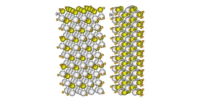
به منظور به دست آوردن ویژگیهای الکترونیکی نانوسیم GaP بدون هرگونه تأثیر سطح، به خاطر حضور باندهای معلق یا خطاهای سطح، ما ابتدا سطح نانوسیم را با اتمهای هیدروژن اشباع می کنیم به طریقی که اتمهای Ga و Pمختصات چهارگانه داشته باشند. نانوسیمهای GaP با اتمهای هیدروژن غیرفعال شده ساختار کریستالی را همچنانکه در شکل 1 می بینیم نشان می دهند، و آنها هیچ سطح انرژی درون یا اطراف شکاف باند نشان نمی دهندبه طور مشابه همانطور که پیشتر برای نانوسیم های InPگزارش کردیم. محاسبات با غیرفعال کردن سطح واقعی تر با Ga2O3 بعدا مورد بحث قرار خواهد گرفت. در ابتدا ما تنها به ساختار الکترونیکی نانوسیم های GaP آغازین به عنوان کارکرد قطرهایشان علاقه مندیم. ما اشکال هندسی چهار نانوسیم که در طول جهت [111] قرار گرفته را بهبود بخشیدیم (شکل (a)1 ) با قطرهای 1.2، 1.7، 2.2، و 2.6 نانومتر در یک سوپرپیل که به ترتیب شامل 68، 116، 176، و 239 اتم می شوند. همچنین دو نانوسیم را که در طول جهت [110]قرار دارد را با قطرهای 0.8 و 1.5 نانومتر که به ترتیب شامل 14 و 40 اتم بودند را مورد بررسی قرار دادیم.
GaP nanowire, a potential material for new devices where optical and electronic applications can be merged, suffers some limitations because it presents indirect band gap. Using first principles calculations we demonstrate that, due to confinement effects, the band gap not only is enlarged when in a nanowire form, but can be transformed to a direct band gap semiconductor nanowire, just by reducing the nanowire diameter to few nanometers. This transition to a direct band gap is obtained for 111 oriented GaP nanowires but not for 110 oriented nanowires. The effects of surface states which can alter the band gap have been studied with hydrogen saturation and an oxide cap layer on the surface of the GaP nanowire. The results show that, while the hydrogen is a perfect passivator, the GaP/Ga2O3 heterojunction presents a small conduction band offset but keeps direct band gap 111 oriented GaP nanowires.
I. INTRODUCTION
III-V semiconductor nanowires have been intensively studied due to their potential applications in optoelectronic devices and photonic circuits.1–3 Gallium phosphide presents so many different nanoscale forms4–7 and, among the different applications, is of particular interesting for miniature optical devices.8 As reported recently9 nanowires of gallium phosphide with few nanometers of diameters can be obtained with very simple techniques, making them useful as building blocks to fabricate nanodevices. However, gallium phosphide presents an indirect band gap of 2.26 eV, which makes it not so useful for optical applications. The generation of light can only occurs by means of excitons with isoelectronic dopants under uniaxial stress,10 hydrostatic pressure11 or shock compression.12 There is not evidence that nanostructured III-V compounds change the minimum of the conduction band as compared to the bulk ones, but an enlargement of the band gap is observed, due to confinement effects.2,13 Nevertheless extended defects like twinning superlattices have been predicted to transform indirect band gap zinc blended semiconductors to direct ones.14 Recently it has been shown that twinning superlattices can be controlled in InP nanowires by controlling the nanowire morphology.15 And if it could be extended to a indirect band gap semiconductor one would transform it in direct band gap material. However a transition from bulk indirect band gap to a nanoscale direct one, only due to nanoeffects, have not been observed in III-V nanostructures so far.
An important issue to obtain electronic properties in nanoscale semiconductors is the, usually hard to determine experimentally, surface structure of the nanomaterial. In order to avoid the surface effects, it has been shown that an oxide cap layer, usually Ga2O3 coating,8,16,17 let the inner GaP nanowire with very crystalline structure. Actually GaP or Ga2O3 nanostructures can be transformed one to another. GaP nanowires can be synthesized from Ga2O3, 18 as well Ga2O3 nanocrystals can be obtained from GaP nanocrystals.19 Outer Ga2O3 layers can work as a protection cap layer for the GaP nanowires, allowing the use of GaP/Ga2O3 structure for nanodevices at high temperatures. What is no so clear till now is the atomic arrangement at the interface between both structures, how is the consequence on the electronic structure due to an oxide on the surface of a GaP nanowire, and how the confinement effects alter the electronic properties of thin nanowires. Theoretical simulations usually use hydrogens as a passivation mechanism to avoid surface dangling bonds,13 while experimentally hydrogen passivation is not feasible, but surface treatment with acids increases significantly the photoluminescence intensity.
In this work, using first principles calculations, it is demonstrated that the indirect bulk GaP band gap can be transformed to a direct band gap semiconductor, just by reducing the nanowire diameter to few nanometers. It was also studied the effects of surface saturation with hydrogens or an oxide cap layer. The results show that the hydrogen is a perfect passivator, and the core-shell GaP/Ga2O3 heterojunction presents a small conduction band offset, but both keep direct band gap 111 oriented nanowires.
II. METHOD
The total energy calculations have been performed with the density functional theory DFT within the generalized gradient approximation GGA Ref. 21 for the exchangecorrelation potential, where the electron-ion interactions are described by ab initio norm-conserving fully separable Troullier–Martins22 pseudopotentials in the Kleinman– Bylander form.23 The total energy has been obtained by a fully self-consistent calculations by solving the standard Kohn–Shan KS equations. The KS orbitals are expanded using a linear combination of numerical pseudoatomic orbitals, implemented in the SIESTA code.24
In all calculations a split-valence double-zeta quality basis set enhanced with polarization function have been shown to reproduce correctly the valence band and binding energies for both GaP and Ga2O3 systems. The results have been compared to other first principles and experimental results.25,26 To guarantee a good description of the charge density, a cutoff of 170 Ry for the grid integration was used to project the charge density in the real space and to calculate the selfconsistent Hamiltonian matrix elements.
It is well known that standard DFT calculations underestimate band gaps, due to a lower position for the conduction band energies. As we are interested here in energy dispersions of conduction bands, a band gap correction may be necessary in order to avoid any spurious interaction which can alter the conduction band energy. To describe correctly the empty states we also used a self-interaction correction SIC scheme,27 which produces exchange parameters more accurate than standard GGA does. The SIC approach, implemented in the SIESTA code, have been used in some structures in order to confirm the main results, especially in those where we want to well describe the unoccupied bands.
Two types of nanowires have been studied in this work. One is aligned along the 111 direction called here z direction, using the supercell approach, in which the periodicity length along the z direction is a3, where a is the bulk lattice parameter. These 111oriented wires present crystalline structure with six 110 planes forming a hexagonal crosssection on the xy planes. The other type of nanowire is aligned along the 10direction, where the periodicity length is a 2/2. All the geometries were optimized until the remaining forces were less than 0.005 eV/Å. The Brillouin zone was sampled using up to five k-points along the nanowire axis. The bulk GaP band gap obtained using the standard GGA-DFT approximation gives a direct band gap of 2.00 eV and an indirect one of 1.70 eV, while by including the SIC approach we get 2.44 eV and 2.17 eV, respectively. As it is known standard DFT always gives smaller energy gaps, however, the SIC improves the value getting it close to the experimentally 2.78 eV and 2.26 eV for indirect and direct band gap, respectively.
III. RESULTS AND DISCUSSION
In order to obtain the electronic properties of an ideal GaP nanowire without any surface effect, due to the presence of dangling bonds or surface defects, we first saturate the nanowire surface with hydrogen atoms in such way that all Ga and P atoms are fourfold coordinated. The GaP nanowires passivated with hydrogen atoms present crystalline structure as can be seen in Fig. 1, and they do not present any surface energy level inside or around the band gap, similarly as reported before for InP nanowires.28 A calculation with a more realistic surface passivation with Ga2O3 will be discussed later. Initially we are only interested in the electronic structure of pristine GaP nanowires as a function of their diameters. We optimize the geometry of four nanowires aligned along the 111 direction Fig. 1a with diameters of 1.2, 1.7, 2.2, and 2.6 nm, in a supercell containing 68, 116, 176, and 239 atoms, respectively. Also we investigate two nanowires aligned along the 110 direction Fig. 1b with diameters of 0.8 nm and 1.5 nm, containing 14 and 40 atoms, respectively.
1. مقدمه
2. روش
3. بحث و نتایج
منابع
1. INTRODUCTION
2. METHOD
3. RESULTS AND DISCUSSION
References